Tag Archives: ARM

Driving OLED Displays

In a recent project I used a small 128×64 pixel OLED display module. These modules are great because the provide a clear and vivid display while requiring no back lighting. The display I used had a Systech SSD1306 controller fitted. The internet is rife with examples of code for driving these displays so I had it up and running with fairly minimal effort.

Having decided to use these displays on another project I am currently working on I found them on the R/C model site HobbyKing. Turns out the MultiWii flight controller (Arduino based flight controller originally using gyroscopes and accelerometers from the Wii controllers) uses an add-on OLED display module which no surprise features a 128×64 OLED display driven but the SSD1306 controller. As I was already ordering from Hobby King I decided to bundle one in with my order.

When the display arrived I assumed since both modules used the same display drivers the code I had already written would work out of the box. Wrong! Come on things are never that simple. Time to start investigating. First thing was to look at the two displays see how they compare. One thing that strikes you straight away is the lack of components on the new display (yellow PCB) compared with the old display (blue PCB).

Working_labelledWorking display module.
Not_Working_labelled

Not working display module.

Next step was to start reading the data sheet to see how this controller is configured. The pin out for the connections to the display can be seen below. I have also labelled them on the pictures above.

Pin Connection Description
1 N/C No connection. (GND)
2 C2P Charge pump capacitor.
3 C2N Charge pump capacitor.
4 C1P Charge pump capacitor.
5 C1N Charge pump capacitor.
6 VBAT DC/DC converter supply.
7 N/C No connection.
8 VSS Logic ground.
9 VDD Logic power supply.
10 BS0 Protocol select.
11 BS1 Protocol select.
12 BS2 Protocol select.
13 CS Chip select.
14 RESET Driver reset.
15 D/C Data/Command select. In I2C mode, this pin acts as SA0 for slave address selection.
16 R/W Read/Write.
17 E/RD Enable Read/Write.
18 D0 Input/output. When I2Cmode is selected, D0 is theserial clock input SCL.
19 D1 Input/output. When I2Cmode is selected, D2 & D1 should be tired together andserve as SDAout & SDAin.
20 D2 Input/output.
21 D3 Input/output.
22 D4 Input/output.
23 D5 Input/output.
24 D6 Input/output.
25 D7 Input/output.
26 IREF Brightness current reference.
27 VCOMH COM signal high voltage. A capacitor should be connected between this pin and VSS.
28 VCC OEL panel power supply. A stabilization capacitor should be connected between this pin and VSS when the converter is used.
29 VLSS Analog ground.
30 N/C No connection. (GND)

The controller has an internal charge pump regulator circuit for generating the 7.5V required by the display. Two external capacitors are required. These are connected between C1P/C1N and C2P/C2N and can be seen on both displays.

Both VCC and VCOMH have decoupling capacitors down to GND as outlined in the data sheet. The brightness current is set by the resistor between IREF and GND. The working display using 910K while the non working display opting to use 560K. The 3.3V regulator provides the required logic voltage.

Interestingly it turns out the controller supports communication over I2C, SPI (3 and 4 wire) and parallel. The protocol selection pins BS0-BS2 allow different protocols to be selected. Both displays have BS0 and BS2 are tied to GND while BS2 is tied to the positive supply which as expected sets the mode to I2C.

When configured for I2C mode D0 acts as the serial clock input. The data sheet stipulates that D1 and D2 should then be connected together to act as the serial data line. On closer inspection of both displays it becomes apparent this is the case the working display (blue PCB) but not with the non working display (yellow). Another thing the working display appears to have pull up resistors connected to SCL and SDA. Something you would expect with I2C comms. The non working display has no pull ups fitted.

Having said that the non working display appears to have three unpopulated foot prints on the PCB allowing for pull resistors to be fitted and for D1 and D2 to be connected together. So the first I did was to add and a zero ohm link between D1 and D2 joining them together. I didn’t bother with any pull up resistors. After fitting the display back into my development board and powering up to my surprise it worked!!

I can only assume when configured for I2C operation D1 acts as the serial input to the controller while D2 acts as the output. Joining the two must allow the acknowledge bit set by the controller to be read by the driver. The driver could have been modified to remove the need for the acknowledgement but this would have meant changing the code to be device specific which I didn’t want to do.

One nice feature on the old display is the ability to change the slave address. In I2C operation the Data/Command pin can be configured to set the lowest bit of the slave address SA0. Allowing the slave address to be either 0x78 or 0x7A. Meaning more than one display could fitted on the same bus.

Another slight gripe is the lack of power on reset circuitry on the new display. The working display has a simple reset circuit comprising R1, C1 and D9. The RC network ensures the reset pulse is present while the supply voltage rises keeping the controller in reset while the supply stabilises. D9 allows C1 to quickly discharge on power down in order to generate a reset pulse on power up in the case of short power downs or spikes. Having the reset pin tied directly to the supply, in the case of the new display, means the reset pin will rise of the same rate as the supply which is not ideal. The track could be cut and a reset circuit added but since it worked I wasn’t going to start modifying it.


TP-Link WDR4300 Router Recovery

My new wireless router decided to stop working at the weekend. It has been behaving rather strange for the past few days. I’ve tried power cycling in the vain hope a reboot may fix the issue. Which it didn’t. And to make things worse now it wont even boot. Pinging it gets no response either. The original firmware was replaced with DD WRT, a great Linux alternative firmware, so the first thing I did was head over to the DD WRT homepage for help. I tried the recommended 30/30/30 reset procedure which didn’t solve the issue.

Luckily there is a ton of resources out there surrounding these routers. Once such resource I found extremely useful was the OpenWRT Wiki page. Apparently the WDR4300 has an Atheros AR9344 SOC running at 560 MHz with 8MB of flash and 128 MB DRAM. It also has both a JTAG and serial programming/debug connection. The flash memory is made up of the boot loader (U-Boot), the operating firmware and the ART (which contains MAC addresses and calibration data for the wifi). It’s also the boot loaders responsibility for configuring the serial interface.

WDR4300_1With nothing to lose I begun disassembling the router to see if I could get access to this serial port and maybe diagnose the problem. After removing the aerials and the screws holding the case together I had the router disassembled. There are two unpopulated headers one 14 pin, which I assume must be the JTAG connection, and one 4 pin which turns out to be the serial connection. The four pins comprising the two supply lines and the TX and RX lines. I soldered in a pin header to the board and connected my USB to serial converter. The connection settings according to the OpenWRT Wiki page are 115200 8N1 with no flow control. Using puTTY I managed to capture the routers output during power up.

 U-Boot 1.1.4 (Apr 25 2012 - 18:29:12)  
 U-boot DB120  
 DRAM: 128 MB  
 id read 0x100000ff  
 flash size 8MB, sector count = 128  
 Flash: 8 MB  
 Using default environment  
 In: serial  
 Out: serial  
 Err: serial  
 Net: ag934x_enet_initialize...  
 No valid address in Flash. Using fixed address  
 wasp reset mask:c03300  
 WASP ----> S17 PHY *  
 : cfg1 0x7 cfg2 0x7114  
 eth0: ba:be:fa:ce:08:41  
 athrs17_reg_init: complete  
 eth0 up  
 eth0  
 Autobooting in 1 seconds  
 ## Booting image at 9f020000 ...  
 Uncompressing Kernel Image ... OK  
 Starting kernel ...  

The output shows the boot loader initialising the serial port. After initialisation the boot loader attempts to auto boot the image at address 0x9F020000. Firstly by uncompressing the kernel image and then starting it. Additional serial output follows before we encounter a raft of file system page read errors before stopping.

 start service  
 starting Architecture code for wasp  
 [ 1.960000] SQUASHFS error: lzma returned unexpected result 0x1  
 [ 1.960000] SQUASHFS error: Unable to read page, block c523, size dd54  
 [ 2.030000] SQUASHFS error: lzma returned unexpected result 0x1  
 [ 2.030000] SQUASHFS error: Unable to read page, block c523, size dd54  
 [ 2.100000] SQUASHFS error: lzma returned unexpected result 0x1  
 [ 2.100000] SQUASHFS error: Unable to read page, block c523, size dd54  
 [ 2.170000] SQUASHFS error: lzma returned unexpected result 0x1  
 [ 2.170000] SQUASHFS error: Unable to read page, block c523, size dd54  
 [ 2.240000] SQUASHFS error: lzma returned unexpected result 0x1  
 [ 2.240000] SQUASHFS error: Unable to read page, block c523, size dd54  
 [ 2.310000] SQUASHFS error: lzma returned unexpected result 0x1  
 [ 2.310000] SQUASHFS error: Unable to read page, block c523, size dd54  
 [ 2.380000] SQUASHFS error: lzma returned unexpected result 0x1  
 [ 2.380000] SQUASHFS error: Unable to read page, block c523, size dd54  
 [ 2.450000] SQUASHFS error: lzma returned unexpected result 0x1  

So it appears the firmware may have become corrupted. The obvious next step then was to try re-flashing it. After some reading around on the subject (being a complete Linux novice) I discovered the boot loader supports network transfer via the Trivial File Transfer Protocol (TFTP). So it is possible to transfer the firmware image via TFTP and re-flash it.

The first step was to download the required firmware images and other supporting software. I downloaded the DD-WRT firmware image files from here and then downloaded and installed the client side TFTP server program TFTPD32 from here.

The next step was to break execution of the boot loader in order to run tftpboot. To do this, within putty after power cycling, simply wait for the message “Autobooting in 1 second” to appear begin typing “tpl” and pressing enter until the sequence stops and the prompt “db12x>” appears. Once the prompt appeared I ran “tftpboot”. I then made a note of the expected server address “192.168.1.100” and load address “0x81000000”. I then exited tftpboot by pressing Ctrl+C.

 db12x> tftpboot  
 dup 1 speed 1000  
  Warning: no boot file name; using '6F01A8C0.img'  
 Using eth0 device  
 TFTP from server 192.168.1.100; our IP address is 192.168.1.111  
 Filename '6F01A8C0.img'.  
 Load address: 0x81000000  
 Log: *  
 TFTP error: 'Access violation' (2)  
 Starting again  

With the router connected directly via an ethernet cable and all wireless adaptors disabled I set the network adaptor to the static IP address “192.168.1.100”. I then ran TFTPD32, browsed for the folder containing the firmware images and set the server address to “192.168.1.100”.
I then ran “tftpboot” again with required load address and source firmware parameters. The new firmware then begun transferring. Upon completion the message “done” appeared and the number of bytes transferred was shown.

 db12x> tftpboot 0x81000000 factory-to-ddwrt.bin  
 Using eth0 device  
 TFTP from server 192.168.1.100; our IP address is 192.168.1.111  
 Filename 'factory-to-ddwrt.bin'.  
 Load address: 0x81000000  
 Lg: #################################################################  
      #################################################################  
      #################################################################  
      #################################################################  
      #################################################################  
      #################################################################  
      #################################################################  
      #################################################################  
      #################################################################  
      #################################################################  
      #################################################################  
      #################################################################  
      #################################################################  
      #################################################################  
      #################################################################  
      #################################################################  
      #################################################################  
      #################################################################  
      #################################################################  
      #################################################################  
      #################################################################  
      #################################################################  
      #################################################################  
      #################################################################  
      ############################  
 done  
 Bytes transferred = 8126464 (7c0000 hex)  

Before the new firmware image could now be copied the destination flash the destination flash first needed to be erased. The destination address being 0x9F020000 (which we know from the initial captured output) and destination length being the size of the transferred firmware image 0x7C0000 bytes.

 db12x> erase 0x9f020000 +7c0000  
 First 0x2 last 0x7d sector size 0x10000                                                                                                 125  
 Erased 124 sectors  

Once erased the new firmware could then be copied over from the destination flash. Again the destination address being 0x9F020000, the source address being 0x81000000 and the length 0x7C0000 bytes.

 db12x> cp.b 0x81000000 0x9f020000 0x7c0000  
 Copy to Flash... write addr: 9f020000  
 done  

So that all appeared fine all that all that remained was to reboot and hopefully everything would be working.

 db12x> reset  

Much to my relief that appeared to have fixed the issue. The router now booted fine and I was able to access to the DD-WRT web interface. WDR4300_7I then went ahead and performed a web flash using the web flash firmware image file previously downloaded. I am not entirely sure this stage was necessary but some of the guides I had read previously did and I cant imagine it would do any harm doing so.

So overall a great result. Saved myself some money not having to rush out and buy a new router and learnt a little bit about Linux in the process.


Nucleo Mod Player

Found myself with a bit of free time this evening so I decided to port my mod player code over to the STM32 Nucleo F401 development board. I haven’t bothered with a display and rather than using an SD card I have converted a couple of modules (using bin2c) and included them in the code. The HWB on the Nucleo is used to move through the mod files stored in the device.


Having fun with TFT displays

Over the last couple of days I have been somewhat struggling to get a TFT display module I recently purchased from eBay working. There seems to be an abundance of posts littered all over the internet regarding these cheap Chinese TFT displays. The problem seems to be that sellers are miss stating the controller these modules are fitted with.

tft

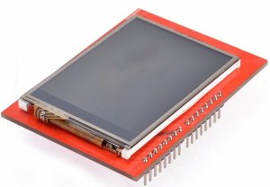
The module I purchased allegedly had an SPFD5408 controller fitted. The reason I went for this module was that it has a Arduino Uno foot print so should be compatible with the Nucleo development board. Another bonus is it also comes with a 4 wire resistive touch screen and micro SD card socket.

Display Connections

TFT Arduino nucLEO
LCD_RST A4 PC_1
LCD_CS A3 PB_0
LCD_RS A2 PA_4
LCD_WR A1 PA_1
LCD_RD A0 PA_0
LCD_D2 D2 PA_10
LCD_D3 D3 PB_3
LCD_D4 D4 PB_5
LCD_D5 D5 PB_4
LCD_D6 D6 PB_10
LCD_D7 D7 PA_8
LCD_D0 D8 PA_9
LCD_D1 D9 PC_7
SD_CS D10 PB_6
SD_DI D11 PA_7
SD_DO D12 PA_6
SD_SCK D13 PA_5

As you can see from the pin out the controller uses an 8 bit parallel interface with a further five dedicated control pins. So using my Nucleo development board I started writing a basic driver, something to simply initialise the display and maybe draw some simple test patterns just so I could confirm it was working.

 void MW_TFT_Init(void)  
 {       
      GPIO_InitTypeDef GPIO_InitDef;  
      uint16_t id;  
      /* Enable LCD control pin clocks */  
      RCC_AHB1PeriphClockCmd(MW_TFT_RST_CLK, ENABLE);  
      RCC_AHB1PeriphClockCmd(MW_TFT_CS_CLK, ENABLE);  
      RCC_AHB1PeriphClockCmd(MW_TFT_RS_CLK, ENABLE);  
      RCC_AHB1PeriphClockCmd(MW_TFT_WR_CLK, ENABLE);  
      RCC_AHB1PeriphClockCmd(MW_TFT_RD_CLK, ENABLE);  
      /* LCD_RST */  
      GPIO_InitDef.GPIO_Pin = MW_TFT_RST_PIN;  
      GPIO_InitDef.GPIO_Speed = GPIO_Speed_50MHz;  
      GPIO_InitDef.GPIO_Mode = GPIO_Mode_OUT;  
      GPIO_InitDef.GPIO_OType = GPIO_OType_PP;  
      GPIO_InitDef.GPIO_PuPd = GPIO_PuPd_NOPULL;  
      GPIO_Init(MW_TFT_RST_PORT, &GPIO_InitDef);  
      /* LCD_CS */  
      GPIO_InitDef.GPIO_Pin = MW_TFT_CS_PIN;  
      GPIO_InitDef.GPIO_Speed = GPIO_Speed_50MHz;  
      GPIO_InitDef.GPIO_Mode = GPIO_Mode_OUT;  
      GPIO_InitDef.GPIO_OType = GPIO_OType_PP;  
      GPIO_InitDef.GPIO_PuPd = GPIO_PuPd_NOPULL;  
      GPIO_Init(MW_TFT_CS_PORT, &GPIO_InitDef);  
      /* LCD_RS */  
      GPIO_InitDef.GPIO_Pin = MW_TFT_RS_PIN;  
      GPIO_InitDef.GPIO_Speed = GPIO_Speed_50MHz;  
      GPIO_InitDef.GPIO_Mode = GPIO_Mode_OUT;  
      GPIO_InitDef.GPIO_OType = GPIO_OType_PP;  
      GPIO_InitDef.GPIO_PuPd = GPIO_PuPd_NOPULL;  
      GPIO_Init(MW_TFT_RS_PORT, &GPIO_InitDef);  
      /* LCD_WR */  
      GPIO_InitDef.GPIO_Pin = MW_TFT_WR_PIN;  
      GPIO_InitDef.GPIO_Speed = GPIO_Speed_50MHz;  
      GPIO_InitDef.GPIO_Mode = GPIO_Mode_OUT;  
      GPIO_InitDef.GPIO_OType = GPIO_OType_PP;  
      GPIO_InitDef.GPIO_PuPd = GPIO_PuPd_NOPULL;  
      GPIO_Init(MW_TFT_WR_PORT, &GPIO_InitDef);  
      /* LCD_RD */  
      GPIO_InitDef.GPIO_Pin = MW_TFT_RD_PIN;  
      GPIO_InitDef.GPIO_Speed = GPIO_Speed_50MHz;  
      GPIO_InitDef.GPIO_Mode = GPIO_Mode_OUT;  
      GPIO_InitDef.GPIO_OType = GPIO_OType_PP;  
      GPIO_InitDef.GPIO_PuPd = GPIO_PuPd_NOPULL;  
      GPIO_Init(MW_TFT_RD_PORT, &GPIO_InitDef);  
      /* Enable LCD data pin clocks */  
      RCC_AHB1PeriphClockCmd(MW_TFT_LCD0_CLK, ENABLE);  
      RCC_AHB1PeriphClockCmd(MW_TFT_LCD1_CLK, ENABLE);  
      RCC_AHB1PeriphClockCmd(MW_TFT_LCD2_CLK, ENABLE);  
      RCC_AHB1PeriphClockCmd(MW_TFT_LCD3_CLK, ENABLE);  
      RCC_AHB1PeriphClockCmd(MW_TFT_LCD4_CLK, ENABLE);  
      RCC_AHB1PeriphClockCmd(MW_TFT_LCD5_CLK, ENABLE);  
      RCC_AHB1PeriphClockCmd(MW_TFT_LCD6_CLK, ENABLE);  
      RCC_AHB1PeriphClockCmd(MW_TFT_LCD7_CLK, ENABLE);  
      /* Set LCD data pins outputs */  
      MW_TFT_SetWriteDirection();  
      /* Set all control lines high */  
      MW_TFT_RST_HIGH;  
      MW_TFT_CS_HIGH;  
      MW_TFT_RS_HIGH;  
      MW_TFT_WR_HIGH;  
      MW_TFT_RD_HIGH;  
      /* Reset TFT */  
      MW_TFT_RST_LOW;  
      Delayms(2);  
      MW_TFT_RST_HIGH;  
      /* Resync */  
      MW_TFT_WriteData(0);  
      MW_TFT_WriteData(0);  
      MW_TFT_WriteData(0);  
      MW_TFT_WriteData(0);  
 }  
 void MW_TFT_WriteData(uint16_t data)  
 {  
      MW_TFT_CS_LOW;  
      MW_TFT_RS_HIGH;  
      MW_TFT_RD_HIGH;  
      MW_TFT_WR_HIGH;  
      /* Send high byte */  
      MW_TFT_Write8(data>>8);  
      MW_TFT_WR_LOW;  
      __asm("nop");  
      MW_TFT_WR_HIGH;  
      /* Send low byte */  
      MW_TFT_Write8(data);  
      MW_TFT_WR_LOW;  
      __asm("nop");  
      MW_TFT_WR_HIGH;  
      MW_TFT_CS_HIGH;  
 }  
 void MW_TFT_WriteCommand(uint16_t cmd)  
 {  
      MW_TFT_CS_LOW;  
      MW_TFT_RS_LOW;  
      MW_TFT_RD_HIGH;  
      MW_TFT_WR_HIGH;  
      /* Send high byte */  
      MW_TFT_Write8(cmd>>8);  
      MW_TFT_WR_LOW;  
      __asm("nop");  
      MW_TFT_WR_HIGH;  
      /* Send low byte */  
      MW_TFT_Write8(cmd);  
      MW_TFT_WR_LOW;  
      __asm("nop");  
      MW_TFT_WR_HIGH;  
      MW_TFT_CS_HIGH;  
 }  
 uint16_t MW_TFT_ReadData(void)  
 {  
      uint16_t data = 0;  
      MW_TFT_CS_LOW;  
      MW_TFT_RS_HIGH;  
      MW_TFT_RD_HIGH;  
      MW_TFT_WR_HIGH;  
      /* Read high byte */  
      MW_TFT_RD_LOW;  
      Delay(10);  
      data = MW_TFT_Read8();  
      data <<= 8;  
      /* Read low byte */  
      MW_TFT_RD_HIGH;  
      MW_TFT_RD_LOW;  
      Delay(10);  
      data |= MW_TFT_Read8();  
      MW_TFT_RD_HIGH;  
      MW_TFT_CS_HIGH;  
      return data;  
 }  
 uint16_t MW_TFT_ReadRegister(uint16_t addr)  
 {  
      MW_TFT_WriteCommand(addr);  
      return MW_TFT_ReadData();  
 }  
 void MW_TFT_WriteRegister(uint16_t addr, uint16_t data)  
 {  
      MW_TFT_WriteCommand(addr);  
      MW_TFT_WriteData(data);  
 }  
 void MW_TFT_SetWriteDirection(void)  
 {  
      GPIO_InitTypeDef GPIO_InitDef;  
      /* LCD_D0 */  
      GPIO_InitDef.GPIO_Pin = MW_TFT_LCD0_PIN;  
      GPIO_InitDef.GPIO_Speed = GPIO_Speed_50MHz;  
      GPIO_InitDef.GPIO_Mode = GPIO_Mode_OUT;  
      GPIO_InitDef.GPIO_OType = GPIO_OType_PP;  
      GPIO_InitDef.GPIO_PuPd = GPIO_PuPd_NOPULL;  
      GPIO_Init(MW_TFT_LCD0_PORT, &GPIO_InitDef);  
      /* LCD_D1 */  
      GPIO_InitDef.GPIO_Pin = MW_TFT_LCD1_PIN;  
      GPIO_InitDef.GPIO_Speed = GPIO_Speed_50MHz;  
      GPIO_InitDef.GPIO_Mode = GPIO_Mode_OUT;  
      GPIO_InitDef.GPIO_OType = GPIO_OType_PP;  
      GPIO_InitDef.GPIO_PuPd = GPIO_PuPd_NOPULL;  
      GPIO_Init(MW_TFT_LCD1_PORT, &GPIO_InitDef);  
      /* LCD_D2 */  
      GPIO_InitDef.GPIO_Pin = MW_TFT_LCD2_PIN;  
      GPIO_InitDef.GPIO_Speed = GPIO_Speed_50MHz;  
      GPIO_InitDef.GPIO_Mode = GPIO_Mode_OUT;  
      GPIO_InitDef.GPIO_OType = GPIO_OType_PP;  
      GPIO_InitDef.GPIO_PuPd = GPIO_PuPd_NOPULL;  
      GPIO_Init(MW_TFT_LCD2_PORT, &GPIO_InitDef);  
      /* LCD_D3 */  
      GPIO_InitDef.GPIO_Pin = MW_TFT_LCD3_PIN;  
      GPIO_InitDef.GPIO_Speed = GPIO_Speed_50MHz;  
      GPIO_InitDef.GPIO_Mode = GPIO_Mode_OUT;  
      GPIO_InitDef.GPIO_OType = GPIO_OType_PP;  
      GPIO_InitDef.GPIO_PuPd = GPIO_PuPd_NOPULL;  
      GPIO_Init(MW_TFT_LCD3_PORT, &GPIO_InitDef);  
      /* LCD_D4 */  
      GPIO_InitDef.GPIO_Pin = MW_TFT_LCD4_PIN;  
      GPIO_InitDef.GPIO_Speed = GPIO_Speed_50MHz;  
      GPIO_InitDef.GPIO_Mode = GPIO_Mode_OUT;  
      GPIO_InitDef.GPIO_OType = GPIO_OType_PP;  
      GPIO_InitDef.GPIO_PuPd = GPIO_PuPd_NOPULL;  
      GPIO_Init(MW_TFT_LCD4_PORT, &GPIO_InitDef);  
      /* LCD_D5 */  
      GPIO_InitDef.GPIO_Pin = MW_TFT_LCD5_PIN;  
      GPIO_InitDef.GPIO_Speed = GPIO_Speed_50MHz;  
      GPIO_InitDef.GPIO_Mode = GPIO_Mode_OUT;  
      GPIO_InitDef.GPIO_OType = GPIO_OType_PP;  
      GPIO_InitDef.GPIO_PuPd = GPIO_PuPd_NOPULL;  
      GPIO_Init(MW_TFT_LCD5_PORT, &GPIO_InitDef);  
      /* LCD_D6 */  
      GPIO_InitDef.GPIO_Pin = MW_TFT_LCD6_PIN;  
      GPIO_InitDef.GPIO_Speed = GPIO_Speed_50MHz;  
      GPIO_InitDef.GPIO_Mode = GPIO_Mode_OUT;  
      GPIO_InitDef.GPIO_OType = GPIO_OType_PP;  
      GPIO_InitDef.GPIO_PuPd = GPIO_PuPd_NOPULL;  
      GPIO_Init(MW_TFT_LCD6_PORT, &GPIO_InitDef);  
      /* LCD_D7 */  
      GPIO_InitDef.GPIO_Pin = MW_TFT_LCD7_PIN;  
      GPIO_InitDef.GPIO_Speed = GPIO_Speed_50MHz;  
      GPIO_InitDef.GPIO_Mode = GPIO_Mode_OUT;  
      GPIO_InitDef.GPIO_OType = GPIO_OType_PP;  
      GPIO_InitDef.GPIO_PuPd = GPIO_PuPd_NOPULL;  
      GPIO_Init(MW_TFT_LCD7_PORT, &GPIO_InitDef);  
 }  
 void MW_TFT_SetReadDirection(void)  
 {  
      GPIO_InitTypeDef GPIO_InitDef;  
      /* LCD_D0 */  
      GPIO_InitDef.GPIO_Pin = MW_TFT_LCD0_PIN;  
      GPIO_InitDef.GPIO_Speed = GPIO_Speed_50MHz;  
      GPIO_InitDef.GPIO_Mode = GPIO_Mode_IN;  
      GPIO_InitDef.GPIO_OType = GPIO_OType_PP;  
      GPIO_InitDef.GPIO_PuPd = GPIO_PuPd_NOPULL;  
      GPIO_Init(MW_TFT_LCD0_PORT, &GPIO_InitDef);  
      /* LCD_D1 */  
      GPIO_InitDef.GPIO_Pin = MW_TFT_LCD1_PIN;  
      GPIO_InitDef.GPIO_Speed = GPIO_Speed_50MHz;  
      GPIO_InitDef.GPIO_Mode = GPIO_Mode_IN;  
      GPIO_InitDef.GPIO_OType = GPIO_OType_PP;  
      GPIO_InitDef.GPIO_PuPd = GPIO_PuPd_NOPULL;  
      GPIO_Init(MW_TFT_LCD1_PORT, &GPIO_InitDef);  
      /* LCD_D2 */  
      GPIO_InitDef.GPIO_Pin = MW_TFT_LCD2_PIN;  
      GPIO_InitDef.GPIO_Speed = GPIO_Speed_50MHz;  
      GPIO_InitDef.GPIO_Mode = GPIO_Mode_IN;  
      GPIO_InitDef.GPIO_OType = GPIO_OType_PP;  
      GPIO_InitDef.GPIO_PuPd = GPIO_PuPd_NOPULL;  
      GPIO_Init(MW_TFT_LCD2_PORT, &GPIO_InitDef);  
      /* LCD_D3 */  
      GPIO_InitDef.GPIO_Pin = MW_TFT_LCD3_PIN;  
      GPIO_InitDef.GPIO_Speed = GPIO_Speed_50MHz;  
      GPIO_InitDef.GPIO_Mode = GPIO_Mode_IN;  
      GPIO_InitDef.GPIO_OType = GPIO_OType_PP;  
      GPIO_InitDef.GPIO_PuPd = GPIO_PuPd_NOPULL;  
      GPIO_Init(MW_TFT_LCD3_PORT, &GPIO_InitDef);  
      /* LCD_D4 */  
      GPIO_InitDef.GPIO_Pin = MW_TFT_LCD4_PIN;  
      GPIO_InitDef.GPIO_Speed = GPIO_Speed_50MHz;  
      GPIO_InitDef.GPIO_Mode = GPIO_Mode_IN;  
      GPIO_InitDef.GPIO_OType = GPIO_OType_PP;  
      GPIO_InitDef.GPIO_PuPd = GPIO_PuPd_NOPULL;  
      GPIO_Init(MW_TFT_LCD4_PORT, &GPIO_InitDef);  
      /* LCD_D5 */  
      GPIO_InitDef.GPIO_Pin = MW_TFT_LCD5_PIN;  
      GPIO_InitDef.GPIO_Speed = GPIO_Speed_50MHz;  
      GPIO_InitDef.GPIO_Mode = GPIO_Mode_IN;  
      GPIO_InitDef.GPIO_OType = GPIO_OType_PP;  
      GPIO_InitDef.GPIO_PuPd = GPIO_PuPd_NOPULL;  
      GPIO_Init(MW_TFT_LCD5_PORT, &GPIO_InitDef);  
      /* LCD_D6 */  
      GPIO_InitDef.GPIO_Pin = MW_TFT_LCD6_PIN;  
      GPIO_InitDef.GPIO_Speed = GPIO_Speed_50MHz;  
      GPIO_InitDef.GPIO_Mode = GPIO_Mode_IN;  
      GPIO_InitDef.GPIO_OType = GPIO_OType_PP;  
      GPIO_InitDef.GPIO_PuPd = GPIO_PuPd_NOPULL;  
      GPIO_Init(MW_TFT_LCD6_PORT, &GPIO_InitDef);  
      /* LCD_D7 */  
      GPIO_InitDef.GPIO_Pin = MW_TFT_LCD7_PIN;  
      GPIO_InitDef.GPIO_Speed = GPIO_Speed_50MHz;  
      GPIO_InitDef.GPIO_Mode = GPIO_Mode_IN;  
      GPIO_InitDef.GPIO_OType = GPIO_OType_PP;  
      GPIO_InitDef.GPIO_PuPd = GPIO_PuPd_NOPULL;  
      GPIO_Init(MW_TFT_LCD7_PORT, &GPIO_InitDef);  
 }  
 void MW_TFT_Write8(uint8_t data)  
 {  
      if( data & 0x80 ) MW_TFT_LCD7_HIGH;  
      else MW_TFT_LCD7_LOW;  
      if( data & 0x40 ) MW_TFT_LCD6_HIGH;  
      else MW_TFT_LCD6_LOW;  
      if( data & 0x20 ) MW_TFT_LCD5_HIGH;  
      else MW_TFT_LCD5_LOW;  
      if( data & 0x10 ) MW_TFT_LCD4_HIGH;  
      else MW_TFT_LCD4_LOW;  
      if( data & 0x08 ) MW_TFT_LCD3_HIGH;  
      else MW_TFT_LCD3_LOW;  
      if( data & 0x04 ) MW_TFT_LCD2_HIGH;  
      else MW_TFT_LCD2_LOW;  
      if( data & 0x02 ) MW_TFT_LCD1_HIGH;  
      else MW_TFT_LCD1_LOW;  
      if( data & 0x01 ) MW_TFT_LCD0_HIGH;  
      else MW_TFT_LCD0_LOW;  
 }  
 uint8_t MW_TFT_Read8(void)  
 {  
      uint8_t data = 0;  
      if( MW_TFT_LCD7_STATE ) data |= 0x80;  
      if( MW_TFT_LCD6_STATE ) data |= 0x40;  
      if( MW_TFT_LCD5_STATE ) data |= 0x20;  
      if( MW_TFT_LCD4_STATE ) data |= 0x10;  
      if( MW_TFT_LCD3_STATE ) data |= 0x08;  
      if( MW_TFT_LCD2_STATE ) data |= 0x04;  
      if( MW_TFT_LCD1_STATE ) data |= 0x02;  
      if( MW_TFT_LCD0_STATE ) data |= 0x01;  
      return data;  
 }  

Display Initialisation

I find the biggest issue with any TFT display module is initialisation. There are normally a whole host of registers within the controller which need setting up before you can start writing to the display. Now I am not a big fan of datasheets. They are a necessary evil in my opinion. Some times you have no choice. But if I can figure things out without having to refer to a couple of thousand pages a broken English then all the better.

With that in mind I did a quick search for the controller supposedly fitted to the module, hoping to find example code or maybe an Arduino sketch which I could extract the initialisation sequence from. To cut a long story short I ported sequences from numerous sources trying to get this module working to no avail. Rather worryingly it was looking like I may have to start referring to the datasheet for help after all.

Then by chance I stumbled upon an Arduino sketch which had a simple driver check built in. It turns out the first register (index 0) in these controllers often contains a controller ID. Reading this register resulted in the ID 0x7783 being returned. Now from previous hunting around I know a common controller used on these cheap TFT display modules is the ST7783. Surely it couldn’t be that simple right? Well turns out it was that simple. Armed with this information I found a sample initialisation sequence and surprise surprise the display now initialises perfectly.

 void MW_TFT_SendInitSequence2(void)  
 {  
      MW_TFT_WriteRegister(0x00FF, 0x0001);  
      MW_TFT_WriteRegister(0x00F3, 0x0008);  
      MW_TFT_WriteCommand(0x00F3);  
      MW_TFT_WriteRegister(0x0001, 0x0100);  
      MW_TFT_WriteRegister(0x0002, 0x0700);  
      MW_TFT_WriteRegister(0x0003, 0x1030);  
      MW_TFT_WriteRegister(0x0008, 0x0302);  
      MW_TFT_WriteRegister(0x0009, 0x0000);  
      MW_TFT_WriteRegister(0x0010, 0x0000);  
      MW_TFT_WriteRegister(0x0011, 0x0007);  
      MW_TFT_WriteRegister(0x0012, 0x0000);  
      MW_TFT_WriteRegister(0x0013, 0x0000);  
      Delay(1000);  
      MW_TFT_WriteRegister(0x0010, 0x14B0);  
      Delay(500);  
      MW_TFT_WriteRegister(0x0011, 0x0007);  
      Delay(500);  
      MW_TFT_WriteRegister(0x0012, 0x008E);  
      MW_TFT_WriteRegister(0x0013, 0x0C00);  
      MW_TFT_WriteRegister(0x0029, 0x0015);  
      Delay(500);  
      MW_TFT_WriteRegister(0x0030, 0x0000);  
      MW_TFT_WriteRegister(0x0031, 0x0107);  
      MW_TFT_WriteRegister(0x0032, 0x0000);  
      MW_TFT_WriteRegister(0x0035, 0x0203);  
      MW_TFT_WriteRegister(0x0036, 0x0402);  
      MW_TFT_WriteRegister(0x0037, 0x0000);  
      MW_TFT_WriteRegister(0x0038, 0x0207);  
      MW_TFT_WriteRegister(0x0039, 0x0000);  
      MW_TFT_WriteRegister(0x003C, 0x0203);  
      MW_TFT_WriteRegister(0x003D, 0x0403);  
      MW_TFT_WriteRegister(0x0050, 0x0000);  
      MW_TFT_WriteRegister(0x0051, st7783Properties.width - 1);  
      MW_TFT_WriteRegister(0x0052, 0X0000);  
      MW_TFT_WriteRegister(0x0053, st7783Properties.height - 1);  
      MW_TFT_WriteRegister(0x0060, 0xa700);  
      MW_TFT_WriteRegister(0x0061, 0x0001);  
      MW_TFT_WriteRegister(0x0090, 0X0029);  
      MW_TFT_WriteRegister(0x0007, 0x0133);  
      Delay(500);  
      MW_TFT_WriteCommand(0x0022);  
 }  

So the moral of this story don’t always believe everything you read especially on eBay.
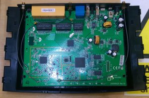
Welcome to the Cube

So continuing my adventure with the new STM32Nucleo development board I began playing around with the STM32CubeMX code generator today. STM32CubeMX is a graphical software configuration tool that allows you to generate initialization code using a graphical wizard.

STM32CubeMXWith today’s microcontrollers becoming more and more advanced and offering multiple functionality it can often take a substantial amount of time just getting up and running. It seems most manufacturers these days offer some form of graphical code generation tool. Texas Instruments have their Pinmux utility,  Renesas have their Appilet tool and ST are no exception with their offering for the STM32 range STM32CubeMX.

The tool is fairly intuitive but like any other tool there is always a learning curve. I found few areas where I came slightly unstuck which was not necessarily any fault of the tool but with configuring the resulting project.

Generating and building a demo project

As a quick guide I intend going through creating an example project with STM32CubeMX and running it on the STM32Nucleo development board. I’ll keep the project simple and in keeping with recent projects we will simply toggle the LED. Since FreeRTOS is a middleware option we will use that as well.

  1. Download and install STM32CubeMX from the link here.
  2. Launch STM32CubeMX and you will be greeted with something similar to that show above.
  3. Click “New Project” project. You can select your processor you wish to use. You can use the drop down boxes to narrow your search or simply check the peripherals you require under the “Peripheral Selection” pane and only MCUs supporting those peripherals will be shown.
  4. Since we will be using the ST32NucleoF401RE board then it’s far simpler just to select it from the “Board Selector” tab.STM32CubeMX_edit
  5. The main window will now show a diagram of your chosen MCU along with the supported peripherals. You will notice that some of the pins have already been assigned signals. Example PA5 the GPIO pin LED LD2 is connected. Also PC13 which is connected to the blue push button. Other pins such as PA2 and PA3 are coloured orange. These pins are are used by USART2 which by default has no mode configured. Some peripherals may have symbols next to them indicating there is currently a conflict or issue with them. Hovering over these peripherals should show more information.
  6. Expand “USART2” by clicking on the “+” next to it. Set the mode to “Asynchronous”. Leave flow control disabled.
  7. Expand “RCC”. Set both the High and Low Speed Clocks to “Crystal/Ceramic Resonator”.
  8. Expand “FREERTOS”  and enable it.
  9. Click the “Clock Configuration” tab. The default configuration should be fine. The clock source should be the 16 MHz HSI RC resonator connected through the PLL Source Mux. /M divide by 16, *N multiply by 336, /P divide by 4. The System Clock Mux should be set to PLLCLK resulting in a SSYCLK of 84 Mhz. AHB Prescaler should be divide by 1, APB1 should be set to divide by 2 and APB2 divide by 1. The end result being an FCLK of 84 MHz.
  10. Next click the “Configuration” tab. You should have FREERTOS, RCC, SYS, and USART2 all enabled.
  11. Save the project settings by either clicking the disk icon in the tool bar.
  12. Start the code generator by clicking the gear icon in the tool bar.
  13. Enter a project name and choose a suitable location to save the generated files.
  14. Select the “MDK-ARM” as the desired tool chain.
  15. Click on “OK” start code generation. When complete close STM32CubeMX.
  16. Open Keil uVision and then load your newly generated project.
  17. Select “Select Device for Target…” from the Project menu.
  18. Type “STM32F401RET” into the search box. The only MCU shown appear is the “STM32F401RET”. Select it and press “OK”.
  19. Select “Rebuild all target files” from the Project menu to rebuild the entire project. It should build successfully with no errors and no warnings.

Modifying the demo project to do something

STM32CubeMX generates quite a few files. The tool embeds a series specific software platform which includes an STM32 abstraction layer to provide an API for accessing the STM32 peripherals. This is all added to the project when created. Again this appears to be something most micro controller manufacturers are doing these days.

So getting back to the code. Referring to the main() function in main.c the functions starts with a number of initialisation functions, the creation of a new thread “StartThread”, followed by a call to start the scheduler (FreeRTOS) and finally an infinite loop. At this point the scheduler is now in control of the program flow.

We only have one thread in this example “StartThread” so let’s modify it to toggle the LED LD2 every 500ms. Make the following changes to “StartThread” function as shown below :-

 static void StartThread(void const * argument)  
 {  
    /* USER CODE BEGIN 5 */  
    /* Infinite loop */  
    for(;;)  
    {  
       HAL_GPIO_TogglePin(GPIOA, GPIO_PIN_5);  
       osDelay(500);  
    }  
    /* USER CODE END 5 */   
 }  

This function now contains all call to HAL_GPIO_TogglePin() which is API hardware call that as its name suggests simply toggles an GPIO pin. In this case pin 5 (GPIO_PIN_5) on general purpose I/O port A (GPIOA). After toggling the pin the function simply waits for 500 ms before repeating the process. Build the target and it should build successfully with no errors and no warnings.

Configuring the debugger

By default ST-Link is not the default debugger for generated project so you will need to configure it before you can successfully execute the project on target.

  1. Connect the STM32Nucleo board to your PC via CN1.
  2. Select “Options For Target” from the Project menu.
  3. Click the “Debug” tab to configure the debugger.target_config1
  4. Select “ST-Link Debugger” as the required debugger.
  5. Click the “Settings” next to the debugger selection.
  6. Select “SW” under the Port setting. The device should now be shown in the SWDIO box.target_config2
  7. Change the “Max Clock” to 4MHz.
  8. Click the “Flash Download” tab.target_config3
  9. Click the “Add” button.
  10. Select “STM32F4xx 512kB Flash” and press “Add”.
  11. OK all open dialogs to return back to the IDE main page.
  12. Select “Start/Stop Debug Session” from the Debug menu.
  13. The project will be download to the STM32Nucleo board and the debugger started. The debugger will then break on the first instruction in the function main().
  14. Press F5 project will begin executing and with any luck LED LD2 should be flashing away.

So there you have it concept to working prototype in next to no time. Well not quite but you can see how STM32CubeMX takes a lot of the initial pain out of configuring your hardware when starting from scratch. The resulting code may be bloated using the HAL and there may not be an abundance of information detailing the use of the HAL but it sure beats trudging through endless pages of the datasheet.

STM32 Nucleo Hello World…Part 2

So after successfully managing to get a simple hello work program up and running on my new STM32 Nucleo development board using mbed I decided I would try some of the other tool chains available. Don’t get me wrong mbed is an awesome platform and offers some really great features but when it comes to development I want to get down and dirty with the micro controller and mbed doesn’t offer that flexibility.

There are a number of other tool chains that support the nucleo boards including IAR Embedded Workbench for ARM from IAR Systems,  Microcontroller Development Kit for ARM from Keil and TrueSTUDIO from Atollic. Not sure about TrueSTUDIO but both EWARM and MDK-ARM are available as free 32K code limited versions. This should be more than enough for modest developments. There are other limitations. I don’t think the limited version of EWARM offers any optimization for instance but I can live with that.

Because I use IAR Embedded Workbench a lot at work (not the ARM version I might add) I decided to try out the Keil MDK-ARM tool chain to see how it compares with the IARs. Below are the steps I took to install it and get the blinky example up and running.

Installing Keil MDK-ARM

  1. Firstly download and install the latest version of MDK-ARM from here. You will need to fill in a few details before downloading but you wont need to apply for a evaluation license.
  2. After the installation has completed launch the newly installed Keil uVision IDE.
  3. Next you need to make sure the middle ware and other packages are up to date. Go to the “Project” menu, select “Manage” and then “Pack Installer”.
  4. Select the “Boards” tab on the right hand side and highlight the “NUCLEO-F401RE” board.
  5. A list of available packs should now appear on the left hand side.
  6. To update the packs click on the install button in the “Action” column of each pack in turn. Ensure the following are up to date. “ARM::CMSIS”, “Keil::MDK-Middleware”, “Keil::STM32F4xx_DFP” and “Keil::STM32NUCLEO_BSP”.
    keil_mdk2
  7. When complete close the pack installer.

Install the STLink USB driver

If you haven’t already done so you will need to download and install the STLink/V2-1 USB drivers from here.

Upgrade STLink

Although not essential its probably a good idea to update the STLink firmware on the STM32 Nucleo board to the latest version by downloading and running the STLink upgrade tool here.

  1. Connect your STM32 Nucleo board to your PC via the USB connector CN1.
  2. Run ST-LinkUpgrade.exe.
  3. Press the “Device Connect” button to connect to your STM32 Nucleo board.
  4. The current firmware version should be displayed and if older than the latest version the message “Upgrade the firmware to VX.XXX.XX” should be shown.stlink_upgrade
  5. Click “Yes>>>>” to perform the upgrade.

Copy the Blinky example

  1. Open the Keil uVision IDE and go to the “Project” menu, select “Manage” and then “Pack Installer”.
  2. Select the “Boards” tab on the right hand side and highlight the “NUCLEO-F401RE” board.
  3. Select the “Examples” tab on the left hand side. The “Blinky” example should appear.
  4. Under the action tab click “Copy” to copy the blinky example project. You will need to provide a path to the destination folder.Blinky
  5. Uncheck the option “Launch uVision” to avoid relaunching the IDE since it is already open.
  6. Press the “OK” button and then close the pack installer.
  7. Open the example project by going to the “Project” menu, select “Open Project…” and navigating to your destination folder. Navigate to the “Blinky” project.
  8. Select and open the Keil uVision project file “Blinky.uvprojx”.
  9. The project will be opened and the “Project” pane on the left hand side should show all of the individual files grouped into folders.Blinky_Project
  10. Go to the “Project” menu and select “Rebuild all targets… ” to build the project. Assuming everything is set up correctly this should build with no errors and no warnings.
  11. Connect your STM32 Nucleo board to your PC via the USB connector CN1.
  12. Go to the “Debug” menu and select “Start/Stop Debug Session”. The generated image will now be programmed to the board.
  13. The debugger will now break at the start of the program (the first instruction in main()  which in this case is initialise the variable num with -1).
  14. Press F5 to start execution. LED “LD2” on the STM32 Nucleo board should start flashing. Using a terminal program connected to the enumerated COM port at 115200 you should also see the phrase “Hello World” being continually output.

So my first outing with the Keil MDK-ARM tool chain has been a success. First impressions of the IDE are very good. Well laid out and reasonably intuitive. However only once you start using a tool in anger do you start to realise its strengths and weaknesses so I guess only time will tell.

STM32 Nucleo Hello World

So managed to grab a bit of time to play with my new STM32 Nucleo development board yesterday. Just as everyone does when they get a new development board I started with the obligatory “Hello World” application. Now because these boards have mbed support and because I had never used mbed before I decided to give it a try.

For those people who have no idea what mbed is. The mbed platform is a free on-line development environment  for the 32 bit ARM Cortex-M range of microcontrollers. Code is written and compiled in this web based IDE. The IDE provides a private workspace with the ability to quickly import and share code with other mbed users. The mbed SDK provides a C/C++ software platform for creating firmware to run on your device. The SDK also provides a library of components that may be used in your own developments.

For anyone who’s interested I’ll quickly go through the steps I took to get the board up and running. Before getting started its probably a good idea to install the ST-Link USB drivers because these will be needed when you first plug in the board.

OK so you have the drivers installed lets get started :-

  1. Firstly you will need to create yourself an mbed developer account at developer.mbed.org/.
  2. Once registered and logged in click on the “Platform” button at the top of the developer page. Select your board, in my case the ST Nucleo F401RE. After selecting the board a detailed description page will open. Simply click “Add to your Compiler” to add this platform to your dashboard.
  3. Next click the “Open mbed Compiler” button to open the online compiler.
  4. Click “Import” to import an example project into your dashboard.
  5. Enter “nucleo” into the search box and click the search button. This should return a number of results.
  6. Highlight the “Nucleo_blink_led” program and click “Import!”. The import dialogue window will open. Leave these settings and press “Import” to continue importing the example program into “My programs”.
  7. To view the code click “main.cpp” to show it in the editor. So as you can see this is pretty noddy stuff. All the program does is turn the LED on for 200 ms and then off for a further second before repeating the process indefinitely.mbed_edit
  8. Click the “Compile” button to build the example program.
  9. The resulting binary image can now be downloaded directly to your device. The program will begin executing immediately.nucleo_drive_edit

So even from this basic example its clear to see mbed offers an extremely fast development path. Design concepts can be realised with minimal effort in next to no time. This example may only flash an LED but the principles are the same.

Not another development board

I fear I am suffering an addiction. An addiction to buying development boards. With ARM appearing to take over the world every manufacturer worth its salt seems to be introducing new ARM based development boards. On a recent spending spree on Farnell a new line of STM32 based boards caught my eye. The STM32 Nucleo range offers a great way to try these powerful micro controllers and comes in numerous flavours. One feature of these boards is that they are mbed compliant allowing for fast development with the on-line development environment. MFG_NUCLEOAnother great feature is that they come fitted with arduino headers so you can use any existing  arduino shields you have laying around. An integrated ST-Link debugger/programmer comes as standard so there is no need for any external tools. Supported development environments for these boards include IAR EWARM, Keil MDK, mbed and GCC based IDEs such as Atollic TrueStudio.

I opted for the STM32F401 one of the high powered variants. The STM32F401 comes fitted with a Cortex-M4 micro controller running at 84 MHz, has 512 kB of flash and bags of I/O including 4 dedicated SPIs. Can’t wait to start playing around with this board stay tuned for more updates.