Tag Archives: Microcontroller

GPS Data Logging

Over the last few weeks I have been playing with a couple of U-Blox NEO-6 Global Positioning System (GPS) receivers I purchased from eBay. What I love about these receivers is they are extremely easy to use. Once powered is applied the receiver starts outputting positional information. The two receivers I have both use a UART interface. However I believe the chip set does support other interfaces including SPI and USB.

Support for these receivers from U-Blox is second to none. As well as a comprehensive manual U-Blox also provide free evaluation software known as U-Center which allows you to evaluate and test these modules in real time. The receivers may also be configured using U-Center.

By the time I received the receivers I already had a couple of projects I wanted to use them for. First off I wanted to build a standalone GPS display device similar to the Quanum GPS Logger V2. The main use for these appears to be for carrying out speed runs of radio controlled cars and planes. Although not massively expensive I figured it would be much more fun to build something similar rather than going out and buying one.

Secondly I wanted a dedicated GPS logging device. As I keen cyclist I am regularly out and about on my mountain bike and often find myself off the beaten track in the middle of nowhere. What would be nice would be the ability to record these routes and import them into Google Earth when I return home. Of course I can track these routes on my phone using Strava or My Tracks but I wanted something a bit more robust. Something I wasn’t overly worried about getting damaged.

Reinventing the Wheel

As I have already mentioned the NEO-6 receivers output positional information via a serial interface. They support two protocols a propriety binary protocol and the National Marine Electronics Association (NMEA) standard. The NMEA standard uses a simple ASCII protocol to send sentences to listening devices. The typical baud rate for this protocol being 4800 baud however my receivers came preconfigured to use 9600 baud. The default update rate for these receivers is every second which is more than adequate for logging purposes.

When it comes to importing this information fortunately Google Earth is now able to import NEMA logs directly without the need for conversion. In the past NEMA logs would have to have been converted to Keyhole Markup Language (KML) format in order to use them with Google Earth. Thankfully this is no longer the case.

So with the receiver continually outputting NMEA messages all that was required was the ability to capture these messages and save them to external media. Now there is no point reinventing the wheel and I figured there must be a whole host of data loggers out there cable of logging serial data. Sparkfuns OpenLog seemed like the ideal solution. OpenLog is an open source Arduino based data logger. Running on an ATMega328 micro controller OpenLog stores received data to an external microSD card. Cards up to 64GB are supposedly supported.

Rather than buying an OpenLog module I built one using a Arduino Nano and a microSD card breakout board. Worked out a lot cheaper in the end. The serial output from the GPS receiver was then fed directly into the Arduino Nano UART RX pin. I did make one minor change to the original OpenLog sketch. By default OpenLog creates new files with the “.TXT” extension. I changed this to “.LOG” which is file type Google Earth is looking for when importing logs. The device is powered via the USB connector, I have it attached to a portable USB power bank at the moment.

logger

I have done a couple of test runs with it and it works great I have logged a couple of bikes rides as well as a 300 miles round trip in the car. All of which imported into Google Earth perfectly. All that remains is to get it into a suitable enclosure.


Driving OLED Displays

In a recent project I used a small 128×64 pixel OLED display module. These modules are great because the provide a clear and vivid display while requiring no back lighting. The display I used had a Systech SSD1306 controller fitted. The internet is rife with examples of code for driving these displays so I had it up and running with fairly minimal effort.

Having decided to use these displays on another project I am currently working on I found them on the R/C model site HobbyKing. Turns out the MultiWii flight controller (Arduino based flight controller originally using gyroscopes and accelerometers from the Wii controllers) uses an add-on OLED display module which no surprise features a 128×64 OLED display driven but the SSD1306 controller. As I was already ordering from Hobby King I decided to bundle one in with my order.

When the display arrived I assumed since both modules used the same display drivers the code I had already written would work out of the box. Wrong! Come on things are never that simple. Time to start investigating. First thing was to look at the two displays see how they compare. One thing that strikes you straight away is the lack of components on the new display (yellow PCB) compared with the old display (blue PCB).

Working_labelledWorking display module.
Not_Working_labelled

Not working display module.

Next step was to start reading the data sheet to see how this controller is configured. The pin out for the connections to the display can be seen below. I have also labelled them on the pictures above.

Pin Connection Description
1 N/C No connection. (GND)
2 C2P Charge pump capacitor.
3 C2N Charge pump capacitor.
4 C1P Charge pump capacitor.
5 C1N Charge pump capacitor.
6 VBAT DC/DC converter supply.
7 N/C No connection.
8 VSS Logic ground.
9 VDD Logic power supply.
10 BS0 Protocol select.
11 BS1 Protocol select.
12 BS2 Protocol select.
13 CS Chip select.
14 RESET Driver reset.
15 D/C Data/Command select. In I2C mode, this pin acts as SA0 for slave address selection.
16 R/W Read/Write.
17 E/RD Enable Read/Write.
18 D0 Input/output. When I2Cmode is selected, D0 is theserial clock input SCL.
19 D1 Input/output. When I2Cmode is selected, D2 & D1 should be tired together andserve as SDAout & SDAin.
20 D2 Input/output.
21 D3 Input/output.
22 D4 Input/output.
23 D5 Input/output.
24 D6 Input/output.
25 D7 Input/output.
26 IREF Brightness current reference.
27 VCOMH COM signal high voltage. A capacitor should be connected between this pin and VSS.
28 VCC OEL panel power supply. A stabilization capacitor should be connected between this pin and VSS when the converter is used.
29 VLSS Analog ground.
30 N/C No connection. (GND)

The controller has an internal charge pump regulator circuit for generating the 7.5V required by the display. Two external capacitors are required. These are connected between C1P/C1N and C2P/C2N and can be seen on both displays.

Both VCC and VCOMH have decoupling capacitors down to GND as outlined in the data sheet. The brightness current is set by the resistor between IREF and GND. The working display using 910K while the non working display opting to use 560K. The 3.3V regulator provides the required logic voltage.

Interestingly it turns out the controller supports communication over I2C, SPI (3 and 4 wire) and parallel. The protocol selection pins BS0-BS2 allow different protocols to be selected. Both displays have BS0 and BS2 are tied to GND while BS2 is tied to the positive supply which as expected sets the mode to I2C.

When configured for I2C mode D0 acts as the serial clock input. The data sheet stipulates that D1 and D2 should then be connected together to act as the serial data line. On closer inspection of both displays it becomes apparent this is the case the working display (blue PCB) but not with the non working display (yellow). Another thing the working display appears to have pull up resistors connected to SCL and SDA. Something you would expect with I2C comms. The non working display has no pull ups fitted.

Having said that the non working display appears to have three unpopulated foot prints on the PCB allowing for pull resistors to be fitted and for D1 and D2 to be connected together. So the first I did was to add and a zero ohm link between D1 and D2 joining them together. I didn’t bother with any pull up resistors. After fitting the display back into my development board and powering up to my surprise it worked!!

I can only assume when configured for I2C operation D1 acts as the serial input to the controller while D2 acts as the output. Joining the two must allow the acknowledge bit set by the controller to be read by the driver. The driver could have been modified to remove the need for the acknowledgement but this would have meant changing the code to be device specific which I didn’t want to do.

One nice feature on the old display is the ability to change the slave address. In I2C operation the Data/Command pin can be configured to set the lowest bit of the slave address SA0. Allowing the slave address to be either 0x78 or 0x7A. Meaning more than one display could fitted on the same bus.

Another slight gripe is the lack of power on reset circuitry on the new display. The working display has a simple reset circuit comprising R1, C1 and D9. The RC network ensures the reset pulse is present while the supply voltage rises keeping the controller in reset while the supply stabilises. D9 allows C1 to quickly discharge on power down in order to generate a reset pulse on power up in the case of short power downs or spikes. Having the reset pin tied directly to the supply, in the case of the new display, means the reset pin will rise of the same rate as the supply which is not ideal. The track could be cut and a reset circuit added but since it worked I wasn’t going to start modifying it.


TM1638 Seven Segment Display Driver with Key Scan Interface

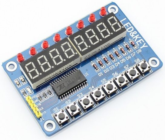
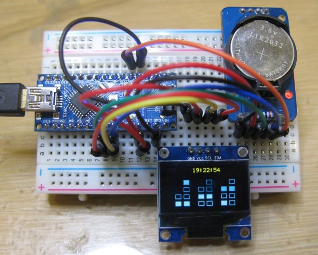
While looking for a new display on eBay recently I stumbled across a seven segment display module. The module (shown below) features 8 seven segment displays, 8 push button switches as well as 8 LEDs. All of which are controlled by one single driver IC the TM1638. I have never come across the TM1638 before, I have used similar display driver ICs like the MAX7219, but never the TM1638.

led_key

After some googling I discovered the TM1638 is manufactured by a Chinese outfit known as Titan Micro Electronics. After downloading the data sheet I begun looking to see how this driver is used. At this point I must state the data sheet, which appears to have been translated from chinese to english, badly, leaves a lot to be desired. Fortunately for me the Arduino fanboys seem to love these devices and there is no shortage of information scattered across the internet. So armed with this information I decided to purchase one.

Once it had arrived getting it working was fairly straight forward. The module does not come with schematic and I wasn’t going to bother reverse engineering the board to create one (not unless I ran into any issues I could not resolve) so it was a bit trial and error in the early stages. In the rest of the post I will demonstrate how to use this device in more detail.

Background

The TM1638 is a LED driver controller with integrated key-scan interface. Communication with the device is via a 3 wire serial interface. The device is capable to of driving up to 8 x 10 LED segments. As well as reading 24 individual key inputs. The display intensity of the LED segments can also be dynamically configured.

Connections

The supply voltage for the device is quoted as 5V ±10% however have seen evidence of people using a 3V3 supply and not having issues.

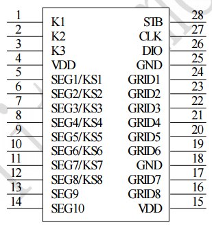
The LED segments are connected to the device via the segment output pins SEG1-SEG10 and grid output pins GRID1-GRID8. The module I purchased has 8 seven segment displays and a further 8 LEDs. These seven segment displays connect via segment output pins SEG1-SEG8 and grid output pins GRID1-GRID8. The 8 LEDs connect via segment output pin SEG9 and grid output pins GRID1-GRID8.

Image17

The push button switches are multiplexed together and read via key state output pins KS1-KS8 and key scan data input pins K1-K3. Note key state output pins KS1-KS8 share the same physical pins as the segment output pins SEG1-SEG8. The device simply alternates between driving the segment outputs and scanning the key input states.

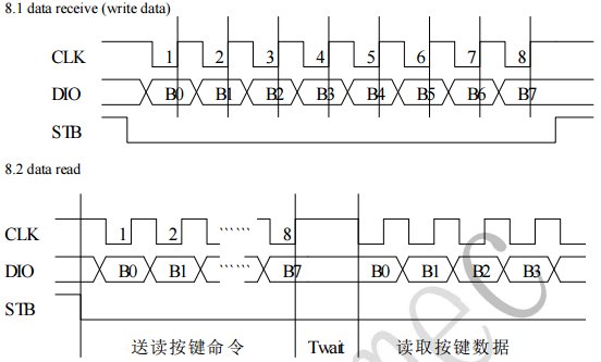
Communication with the device is via a 3 wire serial interface comprising of a strobe (STB), data input/output (DIO) and a clock (CLK) pin. The strobe pin is used to initialise the serial interface prior to sending data. The state of the DIO pin is clocked into the device on the rising edge of the clock signal. Similarly when reading from the device the state of DIO pin may be read on the rising edge of the clock signal.

Image31

Operation

The protocol used to communicate with the TM1638 is a fairly simple one. The transfer is initialised by first pulling the strobe line low, a command byte is then sent followed by a number of optional arguments. The transfer is then terminated by returning the strobe pin high. Each command sent must begin with the strobe pin being pulled low and finish with the strobe pin being pulled high.

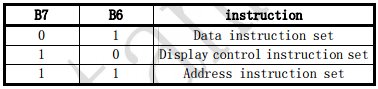
The device supports three command types. Determined by bits B7 and B6 of the command byte. Data instruction set 0b01 (0x4X) writes or reads data to or from the device. Display control instruction set 0b10 (0x8X) configures the device and Address instruction set 0b11 (0xCX) sets the display register address.

Image23

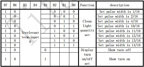
The first thing we want to do post power up is initialise the display. To do so we need to send the display control instruction set command 0x8X.

Image13

The table above shows the individual bit settings for this command and their relevant function. Bits B7 and B6 set the command type, fixed at 0b10 (0x8X). Bits B5 and B4 are irrelevant and set to 0b00. Bit B3 is used to turn the display ON (1) or OFF (0). The remaining bits B2, B1 and B0 configure the display intensity. They actually set the pulse width which determines the display intensity. 1/16 (0x00) being the dullest and 14/16 (0x07) being the brightest.

For instance if we wanted to turn the display ON with the intensity set to maximum we would send the command 0b10001111 (0x8F). For minimum intensity we would send the command 0b10001000 (0x88).

The data instruction set command can perform a number of functions. We can set the data write mode to either write data to a data register or read the key scan data. We can set the address add mode to either automatically increment the destination address while writing data or write to a fixed destination address. There is also a test mode set function which we will not cover here.

Image24

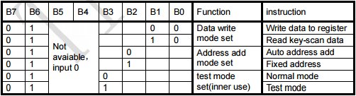
Bits B7 and B6 set the command type and are fixed at 0b01 (0x4X). Bits B5 and B4 are irrelevant and set to 0b00. Bit B3 is used to set the test mode which we will keep set to 0 normal mode. Bit B2 sets the address add mode (0 automatically increments the address and 1 sets a fixed address). Bits B1 and B0 set the data write mode to be either a write to a data register (0b00) or read from the key scan data register (0b10).

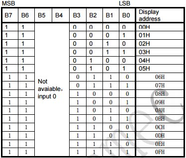
The address instruction set command configures the destination address/register we wish to write. There are 16 display registers in total. Bits B7 and B6 set the command type and are fixed at 0b11 (0xCX). Bits B5 and B4 are irrelevant and set to 0b00. The remaining bits B3, B2, B1 and B0 set the display address (0x00 through 0x0F). The data stored in these registers is used to drive the display segments. Which we will cover in more detail soon.

Image27

This may all look very confusing so let’s cover a couple of examples which should make things a little clearer. Let’s say we want to send the value 0x45 to display register 0x02. The address mode will be fixed since we are only writing one register. So we send the command 0x44 (0b01000100) followed by command 0xC2 (0b11000010) followed by 0x45. If we wanted to send the values 0x01, 0x02 and 0x03 to display registers 0x00, 0x01 and 0x02. The address mode will be set to auto increment since we are writing consecutive registers. We would then send the command 0x40 (0b01000000) followed by command 0xC0 followed by 0x01, 0x02 and 0x03.

To read the state of the keys we need to send the command 0x42 (0b01000010) before reading back 4 bytes containing the key states. The details of which we will cover in more detail further on.

As already mentioned the display registers allow us to set all of the individual segment states. The mapping of each segment in the display registers can be seen in the table below.

Image6

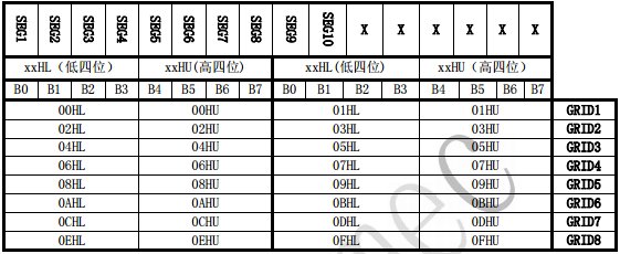
For instance segment output pins SEG1-SEG8 which control the seven segments (A-G) plus the decimal point (DP) on grid output pin GRID1 are mapped to display register 00HL (the lower 4 bits of the display register 0) and 00HU (the upper 4 bits of the display register 0). The remaining two segment output pins SEG9 and SEG10 are mapped to the lower two bits of display register 01HL. The remaining bits of display register 1 have no function. This is then repeated for digit 2 using registers 02HL/02HU and 03HL/03HU etc.

The module I have has single LEDs all connected to segment output pin SEG9 and no connections to segment output pin SEG10. Some of the modules available on eBay have bi-colour LEDs on which I assume SEG9 is used to drive one colour and SEG10 to drive the other.

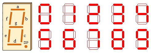
Again this may appear somewhat confusing so let’s have another example. Let’s say we wanted to show ‘0’ on display digit 1. In order to show ‘0’ we need to set segments SEG1 (a), SEG2 (b), SEG3 (c), SEG4 (d), SEG5 (e) and SEG6 (f) while segments SEG7 (g) and SEG8 (DP) remain unset. We do this by loading display register 0 with the value 0b00111111 (0x3F). For display digit 2 we load display register 2 with 0b00111111 (0x3F) etc.

digits

Similarly if we wanted to energise the LED1 we would need to set SEG9 by loading display register 1 with 0b0000001 (0x01). For the LED2 we would load display register 3 with 0b0000001 (0x01) etc.

When it comes to reading the input keys. A maximum of 24 keys may be read by the device. These are all arranged in a 3×8 matrix format. The key states returned from the read key scan data command as four bytes encoded as follows.

Image10

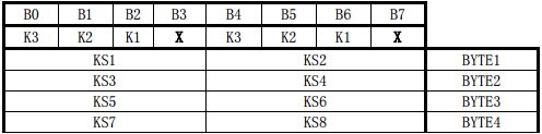
BYTE1 contains the key input states K3 (B0), K2 (B1) and K1 (B2) for key state output KS1 and K3 (B4), K2 (B5) and K1 (B6) for key state output KS2. BYTE2 corresponds to key state outputs KS3 and KS4. BYTE 3 corresponds to key state outputs KS5 and KS6 and BYTE4 corresponds to key state outputs KS7 and KS8. Bits B3 and B7 in all four bytes are irrelevant and are ignored.

For example to read the input state of the key corresponding to input state K2 and key state output KS8 we read bit B5 of BYTE4. To read the input state of the key corresponding to input state K3 and key state output KS1 we read bit B0 of BYTE1.

After a bit of trial and error I discovered the eight keys on my board are all mapped to input state K3. So by checking bits B0 and B4 of each of the 4 bytes read I was able to determine the state of all of the 8 keys.

I have created a basic driver for the TM1638 (written in C) using Atmel Studio. The driver has been tested on a ATMega328 (Arduino Nano) development board. However the code could easily be ported to any other platform if required. All of the project files and an example implementation are all available on my GitHub account.

Binary Clock

For a while now I have fancied building a binary clock. A clock capable of showing the current time in binary format. Not only do they look great but you have the added bonus that most people probably wont have any idea what an earth they are looking at. For those who have no idea what a binary clock is I would highly recommend this Wikipedia page for more information.

To keep things simple I decided on a Binary Coded Decimal (BCD) format rather than pure binary or grey scale. With BCD the hours, minutes and seconds are all represented by individual binary digits. That way you simply add each digit together to determine the number of hours followed by the number of minutes and finally the number seconds.

I wanted something fairly portable, preferably USB powered and reasonably cheap. I ended up using an Arduino Nano clone, a 0.96″ 128×64 OLED display module and a DS3231 real time clock module. This configuration fitted the bill perfectly.

I love these little OLED displays. They are extremely bright and easy to use. The majority if not all of the ones I found on eBay use the SSD1306 display driver chip. The SSD1306 supports a number of interfaces formats including parallel, SPI  and I²C. The module I purchased uses an I²C bus.

The DS3231 I have used on lots of projects before. These devices are extremely accurate with minimal drift over time. Not a lot to say about these really the device maintains seconds, minutes, hours, day, date, month, and year information. Has two configurable alarms and even has an internal temperature sensor (which is used for temperature compensation of the oscillator) but can also be read via one of the internal registers. Data is transferred serially through an I²C bus.

The OLED display supports two colours. The very top of the display uses yellow on black while the remainder of the display uses blue on black. I decided to take advantage of this and alternate between the current time, date and temperature along the top while showing the current time in binary format below using rectangles to represent each binary bit. I am really pleased with the way it turned out.

binary_clock

The design was implemented on breadboard and all of the code written in C using the Atmel Studio development environment. Rather than continually reading the time from the DS3231 its square wave output pin was configured to output a 1Hz square wave which in turn was connected to one of the external interrupts pins on the ATMega328. Upon interrupt the interrupt handler simply sets a flag to indicate to the main exec to read the time and refresh the display. The clock has been running fine now for around four months with no issues at all. All of the project files and source code will be available in my GitHub account.

Arcade Controller Conversion…Part 2

arcade2With the case now modified to fit the new joystick and buttons I moved onto the interface board. Rather than buying one I decided from the onset that I was going to design my own. Those you buy of the shelf in my opinion are just way overpriced for what you get. The majority of which are keyboard encoders. All I needed after all was a simple joystick to USB converter with support for up to eight buttons. The design I came up with encompasses a Minimus AVR development board I already had lying around. These boards are ideal for USB projects. They feature an Atmel  AT90USB162 micro controller with full speed USB controller which makes implementing USB applications a breeze. For the firmware I opted to use the LUFA (Lightweight USB Framework for AVRs, formerly known as MyUSB). I have used LUFA a lot in recent years because I find it extremely easy to implement as well as being extremely well documented.

arcade_controllerWith the design laid out on strip board I started on the firmware. Rather than starting from scratch I took the joystick class driver example provided with the LUFA and begun modifying it to suit my needs. The example project implements a Human Interface Device (HID) class joystick driver. Since most operating systems support the USB HID classes out of the box there is no need for any third party drivers. Within the project is a call back function used to create the HID report to be transferred to the host. All that was needed was, during the call back function, to read the joystick and button states and add them to the generated report. The main USB call would then take care of transferring this report to the host.

 bool CALLBACK_HID_Device_CreateHIDReport( USB_ClassInfo_HID_Device_t* const HIDInterfaceInfo,  
                                           uint8_t* const ReportID,  
                                           const uint8_t ReportType,  
                                           void* ReportData,  
                                           uint16_t* const ReportSize)  
 {  
      /* New joystick report */  
      USB_JoystickReport_Data_t* JoystickReport = (USB_JoystickReport_Data_t*)ReportData;  
      /* Get joystick states */  
      uint8_t JoystickStatus_LCL = ( JOYSTICK_PORT_PIN & JOYSTICK_ALL_MASK ) ^ JOYSTICK_ALL_MASK;  
      /* Get button states */  
      uint8_t ButtonStatus_LCL = ( BUTTONS_PORT_PIN & BUTTONS_ALL_MASK ) ^ BUTTONS_ALL_MASK;  
      /* Check joystick Y axis */  
      if( JoystickStatus_LCL & JOYSTICK_UP_MASK ) JoystickReport->Y = -100;  
      else if( JoystickStatus_LCL & JOYSTICK_DOWN_MASK ) JoystickReport->Y = 100;  
      /* Check joystick X axis */  
      if( JoystickStatus_LCL & JOYSTICK_LEFT_MASK ) JoystickReport->X = -100;  
      else if( JoystickStatus_LCL & JOYSTICK_RIGHT_MASK ) JoystickReport->X = 100;  
      /* Check joystick buttons */  
      if( ButtonStatus_LCL & BUTTONS_BUTTON1_MASK ) JoystickReport->Button |= (1 << 0);  
      if( ButtonStatus_LCL & BUTTONS_BUTTON2_MASK ) JoystickReport->Button |= (1 << 1);  
      if( ButtonStatus_LCL & BUTTONS_BUTTON3_MASK ) JoystickReport->Button |= (1 << 2);  
      if( ButtonStatus_LCL & BUTTONS_BUTTON4_MASK ) JoystickReport->Button |= (1 << 3);  
      if( ButtonStatus_LCL & BUTTONS_BUTTON5_MASK ) JoystickReport->Button |= (1 << 4);  
      if( ButtonStatus_LCL & BUTTONS_BUTTON6_MASK ) JoystickReport->Button |= (1 << 5);  
      if( ButtonStatus_LCL & BUTTONS_BUTTON7_MASK ) JoystickReport->Button |= (1 << 6);  
      if( ButtonStatus_LCL & BUTTONS_BUTTON8_MASK ) JoystickReport->Button |= (1 << 7);  
      /* Set report size */  
      *ReportSize = sizeof(USB_JoystickReport_Data_t);  
      return false;  
 }  

Every USB device must contain an embedded device descriptor which describe to the host information such as what the device is, who makes it, what version of USB it supports etc. This device descriptor contains a vendor ID (a 16-bit number) which is assigned by the USB Implementers Forum to a specific company. Who in turn assign a product ID (again a 16-bit number) to individual products. In the case of the LUFA joystick example the vendor ID and product ID used are 0x03EB and 0x2043 respectively. Refering to the USB ID Repository on the Linux USB home page shows the registered vendor ID as “Atmel Corp.” (no surprise there) and the product ID as “LUFA Joystick Demo Application”. The VID and PID are communicated to the computer when the device is plugged in, along with text strings describing the vendor and product as well as additional descriptors. I choose to modify these vendor and product strings to something more meaningful to me.

output_BGcEfUWith the code compiled and programmed into the AT90USB162 the first test was to check it worked under windows. Once plugged in windows identified the device and installed a suitable driver. Then using the game controllers configuration wizard I was then able to confirm the joystick and buttons were functioning correctly.

Moving on time to start testing on the Raspberry Pi. RetroPie detected the controller and allowed it to be configured for use. This is fine for navigating the RetroPie front end but in order to use it with any of the emulators (apart from MAME who has its own set-up) the controller needs registering for use with RetroArch. So exiting RetroPie and checking available USB devices shows the device has been detected on bus 001 device 005. The vendor ID and product ID clearly shown.

 Bus 001 Device 002: ID 0424:9512 Standard Microsystems Corp.  
 Bus 001 Device 002: ID 0424:9514 Standard Microsystems Corp. 
 Bus 001 Device 001: ID 1d6b:0002 Linux Foundation 2.0 root hub
 Bus 001 Device 003: ID 0424:ec00 Standard Microsystems Corp. 
 Bus 001 Device 004: ID 7392:7811 Edimax Technology Co., Ltd EW-7811Un 802.11n Wireless Adapter [Realtek RTL8188CUS]
 Bus 001 Device 005: ID 03eb:2043 Atmel Corp. LUFA Joystick Demo Application 

Then registering the controller for use with RetroArch using the “Register RetroArch controller” script. You can see the modified manufacturer and product strings read by the script.

  Using joypad: Mikes Modz Arcade Controller  
 Joypads tend to have stale state after opened.  
 Press some buttons and move some axes around to make sure joypad state is completely neutral before proceeding.  
 When done, press Enter ...   
 Configuring binds for player #1 on joypad #0.  
 B button (down)  
      Joybutton pressed: 0  
 Y button (left)  
      Joybutton pressed: 1  
 Select button  
      Joybutton pressed: 2  
 Start button  
      Joybutton pressed: 3  
 Up D-pad  
      Joyaxis moved: Axis 1, Value -32767  
 Down D-pad  
      Joyaxis moved: Axis 1, Value 32767  
 Left D-pad  
      Joyaxis moved: Axis 0, Value -32767  
 Right D-pad  
      Joyaxis moved: Axis 0, Value 32767  
 A button (right)  
      Joybutton pressed: 4  
 X button (top)  
      Joybutton pressed: 5  
 L button (shoulder)  
      Joybutton pressed: 6  
 R button (shoulder)  
      Joybutton pressed: 7  
 L2 button (trigger)  
      Timed out ...  
 R2 button (trigger)  
      Timed out ...  
 L3 button (thumb)  
      Timed out ...  
 R3 button (thumb)  
      Timed out ...  
 Left analog X+ (right)  
      Timed out ...  
 Left analog X- (left)  
      Timed out ...  
 Left analog Y+ (down)  
      Timed out ...  
 Left analog Y- (up)  
      Timed out ...  
 Right analog X+ (right)  
      Timed out ...  
 Right analog X- (left)  
      Timed out ...  
 Right analog Y+ (down)  
      Timed out ...  
 Right analog Y- (up)  
      Timed out ...  
 Writing autoconfig profile to: /opt/retropie/emulators/retroarch/configs/tempconfig.cfg.  
 input_player1_joypad_index = "0"  
 input_player1_b_btn = "0"  
 input_player1_y_btn = "1"  
 input_player1_select_btn = "2"  
 input_player1_start_btn = "3"  
 input_player1_up_axis = "-1"  
 input_player1_down_axis = "+1"  
 input_player1_left_axis = "-0"  
 input_player1_right_axis = "+0"  
 input_player1_a_btn = "4"  
 input_player1_x_btn = "5"  
 input_player1_l_btn = "6"  
 input_player1_r_btn = "7"  
 = = = = = = = = = = = = = = = = = = = = =  
 Configuring RetroArch-AutoConfigs  
 = = = = = = = = = = = = = = = = = = = = =  
 Remapping controller hotkeys  
 Processing /opt/retropie/emulators/retroarch/configs/2Axes11KeysGamePad.cfg  
 Processing /opt/retropie/emulators/retroarch/configs/ControlBlockArcadeGamepad.cfg  
 Processing /opt/retropie/emulators/retroarch/configs/ControlBlockSNESGamepad.cfg  
 Processing /opt/retropie/emulators/retroarch/configs/DragonRise_Inc.___Generic___USB__Joystick__.cfg  
 Processing /opt/retropie/emulators/retroarch/configs/Generic_X-Box_pad.cfg  
 Processing /opt/retropie/emulators/retroarch/configs/GreenAsia_Inc.____USB_Joystick_____.cfg  
 Processing /opt/retropie/emulators/retroarch/configs/HuiJiaSNEStoUSBConverter.cfg  
 Processing /opt/retropie/emulators/retroarch/configs/JessTechColourRumblePad.cfg  
 Processing /opt/retropie/emulators/retroarch/configs/LogitechGamepadF710.cfg  
 Processing /opt/retropie/emulators/retroarch/configs/LogitechLogitechCordlessRumblePad2.cfg  
 Processing /opt/retropie/emulators/retroarch/configs/Logitech_Logitech_Dual_Action.cfg  
 Processing /opt/retropie/emulators/retroarch/configs/Logitech_Logitech_RumblePad_2_USB.cfg  
 Processing /opt/retropie/emulators/retroarch/configs/Microsoft_Sidewinder_Dual_Strike_USB_version_1.cfg  
 Processing /opt/retropie/emulators/retroarch/configs/Microsoft_X-Box_360_pad.cfg  
 Processing /opt/retropie/emulators/retroarch/configs/MikesModzArcadeController.cfg  
 Processing /opt/retropie/emulators/retroarch/configs/MY-POWER_CO__LTD__2In1_USB_Joystick.cfg  
 Processing /opt/retropie/emulators/retroarch/configs/PS3ControllerBT.cfg  
 Processing /opt/retropie/emulators/retroarch/configs/PS3Controller.cfg  
 Processing /opt/retropie/emulators/retroarch/configs/PS3ControllerUSB.cfg  
 Processing /opt/retropie/emulators/retroarch/configs/RockCandyGamepadforPS3.cfg  
 Processing /opt/retropie/emulators/retroarch/configs/Saitek_P880.cfg  
 Processing /opt/retropie/emulators/retroarch/configs/SNES-to-GamepadDevice.cfg  
 Processing /opt/retropie/emulators/retroarch/configs/Sony_PLAYSTATION(R)3_Controller.cfg  
 Processing /opt/retropie/emulators/retroarch/configs/Thrustmaster_Dual_Trigger_3-in-1.cfg  
 Processing /opt/retropie/emulators/retroarch/configs/THRUSTMASTER_FireStorm_Dual_Analog_2.cfg  
 Processing /opt/retropie/emulators/retroarch/configs/Thrustmaster_T_Mini_Wireless.cfg  
 Processing /opt/retropie/emulators/retroarch/configs/USB_2-axis_8-button_gamepad.cfg  
 Processing /opt/retropie/emulators/retroarch/configs/USB_Gamepad.cfg  
 Processing /opt/retropie/emulators/retroarch/configs/USBGamepad.cfg  
 Processing /opt/retropie/emulators/retroarch/configs/Xbox_360_Wireless_Receiver.cfg  
 Processing /opt/retropie/emulators/retroarch/configs/XboxGamepad(userspacedriver).cfg  

With the controller now registered it was time to start playing. First up Teenage Mutant Ninja Turtles on the SNES which worked great. The Seimitsu joystick has a great feel with lovely movement not too stiff but not too loose either. The buttons respond perfectly with minimal effort, if anything they are little bit to sensitive but that’s fine.

Arcade Controller Conversion…Part 1

I love playing retro arcade games and most recently I have taken to playing these classic games on my Raspberry Pi 2 using the RetroPie. For those who aren’t aware the RetroPie project is a collection of works that all have the overall goal to turn the Raspberry Pi into a dedicated retro-gaming console. Up until now I have been using a couple of cheap USB NES controllers. These controllers are great but nothing compares to the feel of an authentic arcade controller. So I set about building my own controller that could be plugged directly into my Raspberry Pi.

arcade4The first issue would be the enclosure. Do I build something? Or do I buy a flat packed kit from eBay? Neither option was going to be cheap. Then I stumbled on someone selling a second hand PlayStation arcade controller on eBay which at the time was listed at 99p plus postage. I figured that has got to be worth a punt. Even if I can only salvage the case and possibly a few other parts then so be it. So I placed a bid and ended up winning it for just over a pound. Result! I wasn’t expecting a lot but was pleasantly surprised when it arrived. The build quality was a lot better than I had expected. It had obviously seen a fair bit of use and the joystick micro switches were worn out. But still I wasn’t disappointed as the case was in great condition.

arcade5I begun disassembling it as soon as it arrived. I removed the bottom plate, the cable, the joystick and the eight push buttons. I had no plans to use the interface board so I de-soldered all of the connections and left the PCB in situ. Next I measured the holes for the push buttons which turned out to be 30mm which was good news since this a standard size for arcade buttons. Selecting a suitable joystick proved to be more troublesome. There isn’t a lot of clearance for the joystick once mounted so I needed to find one with the lowest possible profile.

In the end I went for a Seimitsu LS-58-01and Seimitsu PS-15 buttons. The LS-58 a great quality small form factor joystick. Not to stiff and with an adequate throw distance for my liking. The micro switches are soldered directly into a PCB. This worked out perfect as I later went on to use the PCB to mount it to the original mounting posts. Being 30mm the PS-15’s fitted perfectly with no modifications required. The joystick however required a few modifications. In order to drill the mounting holes in the PCB I first had to remove the common connections for each micro switch. Rather than completely removing the micro switches I simply cut the tabs and de-soldered. Then after drilling the holes I used Kynar wire to re-connect them.

arcade1The next problem was getting the joystick to fit flush with the case. Because of the way the case had been moulded I needed to remove some of the plastic surrounding the stick. Thankfully this didn’t comprise the rigidity of the joystick. The end result wasn’t pretty but at least it now fitted flush with the case. I finished off by connecting all of the switches to my new interface board which I will move onto in the next post.

Welcome to the Cube

So continuing my adventure with the new STM32Nucleo development board I began playing around with the STM32CubeMX code generator today. STM32CubeMX is a graphical software configuration tool that allows you to generate initialization code using a graphical wizard.

STM32CubeMXWith today’s microcontrollers becoming more and more advanced and offering multiple functionality it can often take a substantial amount of time just getting up and running. It seems most manufacturers these days offer some form of graphical code generation tool. Texas Instruments have their Pinmux utility,  Renesas have their Appilet tool and ST are no exception with their offering for the STM32 range STM32CubeMX.

The tool is fairly intuitive but like any other tool there is always a learning curve. I found few areas where I came slightly unstuck which was not necessarily any fault of the tool but with configuring the resulting project.

Generating and building a demo project

As a quick guide I intend going through creating an example project with STM32CubeMX and running it on the STM32Nucleo development board. I’ll keep the project simple and in keeping with recent projects we will simply toggle the LED. Since FreeRTOS is a middleware option we will use that as well.

  1. Download and install STM32CubeMX from the link here.
  2. Launch STM32CubeMX and you will be greeted with something similar to that show above.
  3. Click “New Project” project. You can select your processor you wish to use. You can use the drop down boxes to narrow your search or simply check the peripherals you require under the “Peripheral Selection” pane and only MCUs supporting those peripherals will be shown.
  4. Since we will be using the ST32NucleoF401RE board then it’s far simpler just to select it from the “Board Selector” tab.STM32CubeMX_edit
  5. The main window will now show a diagram of your chosen MCU along with the supported peripherals. You will notice that some of the pins have already been assigned signals. Example PA5 the GPIO pin LED LD2 is connected. Also PC13 which is connected to the blue push button. Other pins such as PA2 and PA3 are coloured orange. These pins are are used by USART2 which by default has no mode configured. Some peripherals may have symbols next to them indicating there is currently a conflict or issue with them. Hovering over these peripherals should show more information.
  6. Expand “USART2” by clicking on the “+” next to it. Set the mode to “Asynchronous”. Leave flow control disabled.
  7. Expand “RCC”. Set both the High and Low Speed Clocks to “Crystal/Ceramic Resonator”.
  8. Expand “FREERTOS”  and enable it.
  9. Click the “Clock Configuration” tab. The default configuration should be fine. The clock source should be the 16 MHz HSI RC resonator connected through the PLL Source Mux. /M divide by 16, *N multiply by 336, /P divide by 4. The System Clock Mux should be set to PLLCLK resulting in a SSYCLK of 84 Mhz. AHB Prescaler should be divide by 1, APB1 should be set to divide by 2 and APB2 divide by 1. The end result being an FCLK of 84 MHz.
  10. Next click the “Configuration” tab. You should have FREERTOS, RCC, SYS, and USART2 all enabled.
  11. Save the project settings by either clicking the disk icon in the tool bar.
  12. Start the code generator by clicking the gear icon in the tool bar.
  13. Enter a project name and choose a suitable location to save the generated files.
  14. Select the “MDK-ARM” as the desired tool chain.
  15. Click on “OK” start code generation. When complete close STM32CubeMX.
  16. Open Keil uVision and then load your newly generated project.
  17. Select “Select Device for Target…” from the Project menu.
  18. Type “STM32F401RET” into the search box. The only MCU shown appear is the “STM32F401RET”. Select it and press “OK”.
  19. Select “Rebuild all target files” from the Project menu to rebuild the entire project. It should build successfully with no errors and no warnings.

Modifying the demo project to do something

STM32CubeMX generates quite a few files. The tool embeds a series specific software platform which includes an STM32 abstraction layer to provide an API for accessing the STM32 peripherals. This is all added to the project when created. Again this appears to be something most micro controller manufacturers are doing these days.

So getting back to the code. Referring to the main() function in main.c the functions starts with a number of initialisation functions, the creation of a new thread “StartThread”, followed by a call to start the scheduler (FreeRTOS) and finally an infinite loop. At this point the scheduler is now in control of the program flow.

We only have one thread in this example “StartThread” so let’s modify it to toggle the LED LD2 every 500ms. Make the following changes to “StartThread” function as shown below :-

 static void StartThread(void const * argument)  
 {  
    /* USER CODE BEGIN 5 */  
    /* Infinite loop */  
    for(;;)  
    {  
       HAL_GPIO_TogglePin(GPIOA, GPIO_PIN_5);  
       osDelay(500);  
    }  
    /* USER CODE END 5 */   
 }  

This function now contains all call to HAL_GPIO_TogglePin() which is API hardware call that as its name suggests simply toggles an GPIO pin. In this case pin 5 (GPIO_PIN_5) on general purpose I/O port A (GPIOA). After toggling the pin the function simply waits for 500 ms before repeating the process. Build the target and it should build successfully with no errors and no warnings.

Configuring the debugger

By default ST-Link is not the default debugger for generated project so you will need to configure it before you can successfully execute the project on target.

  1. Connect the STM32Nucleo board to your PC via CN1.
  2. Select “Options For Target” from the Project menu.
  3. Click the “Debug” tab to configure the debugger.target_config1
  4. Select “ST-Link Debugger” as the required debugger.
  5. Click the “Settings” next to the debugger selection.
  6. Select “SW” under the Port setting. The device should now be shown in the SWDIO box.target_config2
  7. Change the “Max Clock” to 4MHz.
  8. Click the “Flash Download” tab.target_config3
  9. Click the “Add” button.
  10. Select “STM32F4xx 512kB Flash” and press “Add”.
  11. OK all open dialogs to return back to the IDE main page.
  12. Select “Start/Stop Debug Session” from the Debug menu.
  13. The project will be download to the STM32Nucleo board and the debugger started. The debugger will then break on the first instruction in the function main().
  14. Press F5 project will begin executing and with any luck LED LD2 should be flashing away.

So there you have it concept to working prototype in next to no time. Well not quite but you can see how STM32CubeMX takes a lot of the initial pain out of configuring your hardware when starting from scratch. The resulting code may be bloated using the HAL and there may not be an abundance of information detailing the use of the HAL but it sure beats trudging through endless pages of the datasheet.

STM32 Nucleo Hello World…Part 2

So after successfully managing to get a simple hello work program up and running on my new STM32 Nucleo development board using mbed I decided I would try some of the other tool chains available. Don’t get me wrong mbed is an awesome platform and offers some really great features but when it comes to development I want to get down and dirty with the micro controller and mbed doesn’t offer that flexibility.

There are a number of other tool chains that support the nucleo boards including IAR Embedded Workbench for ARM from IAR Systems,  Microcontroller Development Kit for ARM from Keil and TrueSTUDIO from Atollic. Not sure about TrueSTUDIO but both EWARM and MDK-ARM are available as free 32K code limited versions. This should be more than enough for modest developments. There are other limitations. I don’t think the limited version of EWARM offers any optimization for instance but I can live with that.

Because I use IAR Embedded Workbench a lot at work (not the ARM version I might add) I decided to try out the Keil MDK-ARM tool chain to see how it compares with the IARs. Below are the steps I took to install it and get the blinky example up and running.

Installing Keil MDK-ARM

  1. Firstly download and install the latest version of MDK-ARM from here. You will need to fill in a few details before downloading but you wont need to apply for a evaluation license.
  2. After the installation has completed launch the newly installed Keil uVision IDE.
  3. Next you need to make sure the middle ware and other packages are up to date. Go to the “Project” menu, select “Manage” and then “Pack Installer”.
  4. Select the “Boards” tab on the right hand side and highlight the “NUCLEO-F401RE” board.
  5. A list of available packs should now appear on the left hand side.
  6. To update the packs click on the install button in the “Action” column of each pack in turn. Ensure the following are up to date. “ARM::CMSIS”, “Keil::MDK-Middleware”, “Keil::STM32F4xx_DFP” and “Keil::STM32NUCLEO_BSP”.
    keil_mdk2
  7. When complete close the pack installer.

Install the STLink USB driver

If you haven’t already done so you will need to download and install the STLink/V2-1 USB drivers from here.

Upgrade STLink

Although not essential its probably a good idea to update the STLink firmware on the STM32 Nucleo board to the latest version by downloading and running the STLink upgrade tool here.

  1. Connect your STM32 Nucleo board to your PC via the USB connector CN1.
  2. Run ST-LinkUpgrade.exe.
  3. Press the “Device Connect” button to connect to your STM32 Nucleo board.
  4. The current firmware version should be displayed and if older than the latest version the message “Upgrade the firmware to VX.XXX.XX” should be shown.stlink_upgrade
  5. Click “Yes>>>>” to perform the upgrade.

Copy the Blinky example

  1. Open the Keil uVision IDE and go to the “Project” menu, select “Manage” and then “Pack Installer”.
  2. Select the “Boards” tab on the right hand side and highlight the “NUCLEO-F401RE” board.
  3. Select the “Examples” tab on the left hand side. The “Blinky” example should appear.
  4. Under the action tab click “Copy” to copy the blinky example project. You will need to provide a path to the destination folder.Blinky
  5. Uncheck the option “Launch uVision” to avoid relaunching the IDE since it is already open.
  6. Press the “OK” button and then close the pack installer.
  7. Open the example project by going to the “Project” menu, select “Open Project…” and navigating to your destination folder. Navigate to the “Blinky” project.
  8. Select and open the Keil uVision project file “Blinky.uvprojx”.
  9. The project will be opened and the “Project” pane on the left hand side should show all of the individual files grouped into folders.Blinky_Project
  10. Go to the “Project” menu and select “Rebuild all targets… ” to build the project. Assuming everything is set up correctly this should build with no errors and no warnings.
  11. Connect your STM32 Nucleo board to your PC via the USB connector CN1.
  12. Go to the “Debug” menu and select “Start/Stop Debug Session”. The generated image will now be programmed to the board.
  13. The debugger will now break at the start of the program (the first instruction in main()  which in this case is initialise the variable num with -1).
  14. Press F5 to start execution. LED “LD2” on the STM32 Nucleo board should start flashing. Using a terminal program connected to the enumerated COM port at 115200 you should also see the phrase “Hello World” being continually output.

So my first outing with the Keil MDK-ARM tool chain has been a success. First impressions of the IDE are very good. Well laid out and reasonably intuitive. However only once you start using a tool in anger do you start to realise its strengths and weaknesses so I guess only time will tell.

STM32 Nucleo Hello World

So managed to grab a bit of time to play with my new STM32 Nucleo development board yesterday. Just as everyone does when they get a new development board I started with the obligatory “Hello World” application. Now because these boards have mbed support and because I had never used mbed before I decided to give it a try.

For those people who have no idea what mbed is. The mbed platform is a free on-line development environment  for the 32 bit ARM Cortex-M range of microcontrollers. Code is written and compiled in this web based IDE. The IDE provides a private workspace with the ability to quickly import and share code with other mbed users. The mbed SDK provides a C/C++ software platform for creating firmware to run on your device. The SDK also provides a library of components that may be used in your own developments.

For anyone who’s interested I’ll quickly go through the steps I took to get the board up and running. Before getting started its probably a good idea to install the ST-Link USB drivers because these will be needed when you first plug in the board.

OK so you have the drivers installed lets get started :-

  1. Firstly you will need to create yourself an mbed developer account at developer.mbed.org/.
  2. Once registered and logged in click on the “Platform” button at the top of the developer page. Select your board, in my case the ST Nucleo F401RE. After selecting the board a detailed description page will open. Simply click “Add to your Compiler” to add this platform to your dashboard.
  3. Next click the “Open mbed Compiler” button to open the online compiler.
  4. Click “Import” to import an example project into your dashboard.
  5. Enter “nucleo” into the search box and click the search button. This should return a number of results.
  6. Highlight the “Nucleo_blink_led” program and click “Import!”. The import dialogue window will open. Leave these settings and press “Import” to continue importing the example program into “My programs”.
  7. To view the code click “main.cpp” to show it in the editor. So as you can see this is pretty noddy stuff. All the program does is turn the LED on for 200 ms and then off for a further second before repeating the process indefinitely.mbed_edit
  8. Click the “Compile” button to build the example program.
  9. The resulting binary image can now be downloaded directly to your device. The program will begin executing immediately.nucleo_drive_edit

So even from this basic example its clear to see mbed offers an extremely fast development path. Design concepts can be realised with minimal effort in next to no time. This example may only flash an LED but the principles are the same.