In a recent project I used a small 128×64 pixel OLED display module. These modules are great because the provide a clear and vivid display while requiring no back lighting. The display I used had a Systech SSD1306 controller fitted. The internet is rife with examples of code for driving these displays so I had it up and running with fairly minimal effort.
Having decided to use these displays on another project I am currently working on I found them on the R/C model site HobbyKing. Turns out the MultiWii flight controller (Arduino based flight controller originally using gyroscopes and accelerometers from the Wii controllers) uses an add-on OLED display module which no surprise features a 128×64 OLED display driven but the SSD1306 controller. As I was already ordering from Hobby King I decided to bundle one in with my order.
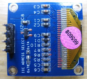
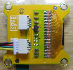
When the display arrived I assumed since both modules used the same display drivers the code I had already written would work out of the box. Wrong! Come on things are never that simple. Time to start investigating. First thing was to look at the two displays see how they compare. One thing that strikes you straight away is the lack of components on the new display (yellow PCB) compared with the old display (blue PCB).
Not working display module.
Next step was to start reading the data sheet to see how this controller is configured. The pin out for the connections to the display can be seen below. I have also labelled them on the pictures above.
| Pin | Connection | Description |
|---|---|---|
| 1 | N/C | No connection. (GND) |
| 2 | C2P | Charge pump capacitor. |
| 3 | C2N | Charge pump capacitor. |
| 4 | C1P | Charge pump capacitor. |
| 5 | C1N | Charge pump capacitor. |
| 6 | VBAT | DC/DC converter supply. |
| 7 | N/C | No connection. |
| 8 | VSS | Logic ground. |
| 9 | VDD | Logic power supply. |
| 10 | BS0 | Protocol select. |
| 11 | BS1 | Protocol select. |
| 12 | BS2 | Protocol select. |
| 13 | CS | Chip select. |
| 14 | RESET | Driver reset. |
| 15 | D/C | Data/Command select. In I2C mode, this pin acts as SA0 for slave address selection. |
| 16 | R/W | Read/Write. |
| 17 | E/RD | Enable Read/Write. |
| 18 | D0 | Input/output. When I2Cmode is selected, D0 is theserial clock input SCL. |
| 19 | D1 | Input/output. When I2Cmode is selected, D2 & D1 should be tired together andserve as SDAout & SDAin. |
| 20 | D2 | Input/output. |
| 21 | D3 | Input/output. |
| 22 | D4 | Input/output. |
| 23 | D5 | Input/output. |
| 24 | D6 | Input/output. |
| 25 | D7 | Input/output. |
| 26 | IREF | Brightness current reference. |
| 27 | VCOMH | COM signal high voltage. A capacitor should be connected between this pin and VSS. |
| 28 | VCC | OEL panel power supply. A stabilization capacitor should be connected between this pin and VSS when the converter is used. |
| 29 | VLSS | Analog ground. |
| 30 | N/C | No connection. (GND) |
The controller has an internal charge pump regulator circuit for generating the 7.5V required by the display. Two external capacitors are required. These are connected between C1P/C1N and C2P/C2N and can be seen on both displays.
Both VCC and VCOMH have decoupling capacitors down to GND as outlined in the data sheet. The brightness current is set by the resistor between IREF and GND. The working display using 910K while the non working display opting to use 560K. The 3.3V regulator provides the required logic voltage.
Interestingly it turns out the controller supports communication over I2C, SPI (3 and 4 wire) and parallel. The protocol selection pins BS0-BS2 allow different protocols to be selected. Both displays have BS0 and BS2 are tied to GND while BS2 is tied to the positive supply which as expected sets the mode to I2C.
When configured for I2C mode D0 acts as the serial clock input. The data sheet stipulates that D1 and D2 should then be connected together to act as the serial data line. On closer inspection of both displays it becomes apparent this is the case the working display (blue PCB) but not with the non working display (yellow). Another thing the working display appears to have pull up resistors connected to SCL and SDA. Something you would expect with I2C comms. The non working display has no pull ups fitted.
Having said that the non working display appears to have three unpopulated foot prints on the PCB allowing for pull resistors to be fitted and for D1 and D2 to be connected together. So the first I did was to add and a zero ohm link between D1 and D2 joining them together. I didn’t bother with any pull up resistors. After fitting the display back into my development board and powering up to my surprise it worked!!
I can only assume when configured for I2C operation D1 acts as the serial input to the controller while D2 acts as the output. Joining the two must allow the acknowledge bit set by the controller to be read by the driver. The driver could have been modified to remove the need for the acknowledgement but this would have meant changing the code to be device specific which I didn’t want to do.
One nice feature on the old display is the ability to change the slave address. In I2C operation the Data/Command pin can be configured to set the lowest bit of the slave address SA0. Allowing the slave address to be either 0x78 or 0x7A. Meaning more than one display could fitted on the same bus.
Another slight gripe is the lack of power on reset circuitry on the new display. The working display has a simple reset circuit comprising R1, C1 and D9. The RC network ensures the reset pulse is present while the supply voltage rises keeping the controller in reset while the supply stabilises. D9 allows C1 to quickly discharge on power down in order to generate a reset pulse on power up in the case of short power downs or spikes. Having the reset pin tied directly to the supply, in the case of the new display, means the reset pin will rise of the same rate as the supply which is not ideal. The track could be cut and a reset circuit added but since it worked I wasn’t going to start modifying it.


