
I often find myself needing a constant current load when testing power supplies, high power LEDs etc. I have thought about building my own for a while now ever since seeing the one Dave Jones built on his EEVblog way back in 2010.
My goal was to design an electronic load capable of sinking a reasonable amount of current, portable so it could be moved around with ease, microprocessor controlled, support constant current, constant power and constant resistance modes. As well as not costing the earth to build.
The design I came up with is relatively simple. Almost all of the component choices are based on what I had lying around. I wasn’t sure at the time how I was going to drive the electronic load so tried to make it generic hence the external ADC and DAC. This way any micro controller with SPI could be used.
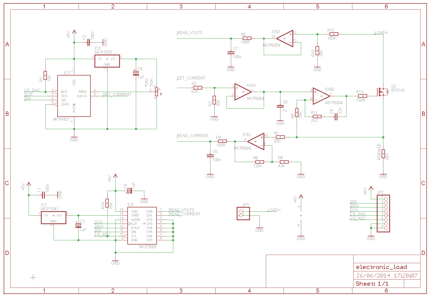 The main current path for the load is through the MOSFET Q1 and the sense resistor Rsense. The amount of current flowing through the load is controlled by adjusting the voltage applied to the gate of Q1. Opamp IC5B is configured as a voltage follower. When a voltage is applied to the non inverting input the opamp will drive Q1s gate voltage to ensure the voltage applied across Rsense is the same as the voltage appearing on the opamps inverting input pin. So applying 1V to the input results in 1V being applied across the sense resistor meaning 10A (1V/0.1R) will be flowing through the load. R11 and C9 provide stability to stop the output from oscillating.
The load current is set by the output of the DAC. I choose the MCP4921 because it has an external reference input. Using an external 2.5V reference and a small trim pot the DAC reference voltage could be adjusted anywhere between 0 and 2.5V. Meaning the maximum load current could be adjusted while still maintaining the resolution. The DAC output voltage is divided by 2 (although looking at the schematic its appears to be divided by 5) before passing through the voltage follower IC5A. Allowing for a maximum load current of around 12.5A.
The load voltage is divided by 9 before passing through the voltage follower IC5D and is then applied the first ADC channel. The ADC has a reference voltage of 4.096V which allows for a maximum load voltage of approximately 36V. I choose to use a MCP3008 ADCs mainly because I had a few lying around. Bit overkill since I only needed 2 channels but the unused channels were simply tied to 0V.
The load current is determined by measuring the voltage across the sense resistor. This voltage is amplified by IC5C and is then applied to the second ADC channel. With a load current of 10A this results in a voltage of around 3.8V.
The FET I choose was a BTS141 smart low side power switch. I could have gone with some other logic level FET or BJT but decided to go with the BTS141 since is has ESD, overload, short circuit and over voltage protection as well as thermal shut-down. I must admit I was a bit paranoid about the FET burning up and figured the extra protection was worth the extra cost.
The next step was to choose a suitable heat sink. The maximum operating temperature of the BTS141 is 150 degrees Celsius. The heat sink I choose to use has a thermal resistance of 2.33 C/W. According to the BTS141 datasheet it has a junction-case thermal resistance of 0.84 C/W. Ignoring the case to heat sink thermal resistance this gives a total thermal resistance of 3.17 C/W. Assuming an ambient temperature of 25 C means the maximum power dissipation would be (150-25)/3.17 = 39W.
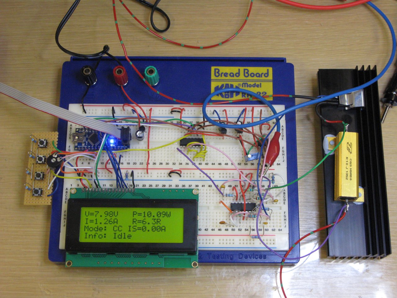
I decided to start building the circuit on breadboard so I could get something up and running as fast a possible. To control the everything I used an Arduino Nano (technically its a copy but hey) with a 4×20 LCD dot matrix display and a few external push buttons.
 The code in the Nano is all written in C. I like the idea of the Arduinos and the relative ease that you can have things up and running but using the Arduino development environment just doesn’t offer the flexibility I want. The Arduinos are a great way of getting a cheap AVR development board and since they all have external ICSP pins you can even erase the bootloader and make use of the entire flash memory.
The software at the moment only supports limited functionality. Which was just so I could test the hardware and calibrate the inputs and outputs. You can see from the picture the circuit working with a load current of a 1.25A @ approx 8V. I have had it running with 10A @ 3V with no issues. The heatsink gets a bit hot but that’s to be expected.
The next stage is to get the final circuit built up and into an enclosure and then finish off the software.
